ST90158 - MULTIPROTOCOL SERIAL COMMUNICATIONS INTERFACE (SCI-M)
MULTIPROTOCOL SERIAL COMMUNICATIONS INTERFACE (Cont’d)
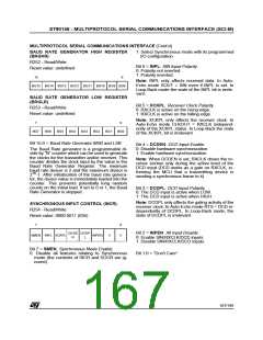
BAUD RATE GENERATOR HIGH REGISTER
(BRGHR)
1: Select Synchronous mode with its programmed
I/O configuration.
R252 - Read/Write
Bit 6 = INPL: SIN Input Polarity.
0: Polarity not inverted.
1: Polarity inverted.
Reset value: undefined
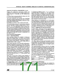
15
8
Note: INPL only affects received data. In Auto-
Echo mode SOUT = SIN even if INPL is set. In
Loop-Back mode the state of the INPL bit is irrele-
vant.
BG15 BG14 BG13 BG12 BG11 BG10 BG9 BG8
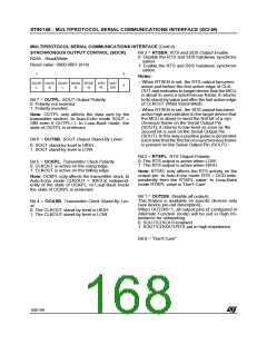
BAUD RATE GENERATOR LOW REGISTER
(BRGLR)
Bit 5 = XCKPL: Receiver Clock Polarity.
0: RXCLK is active on the rising edge.
1: RXCLK is active on the falling edge.
R253 - Read/Write
Reset value: undefined
Note: XCKPL only affects the receiver clock. In
Auto-Echo mode CLKOUT = RXCLK independ-
ently of the XCKPL status. In Loop-Back the state
of the XCKPL bit is irrelevant.
7
0
BG7
BG6
BG5
BG4
BG3
BG2
BG1
BG0
Bit 15:0 = Baud Rate Generator MSB and LSB.
Bit 4 = DCDEN: DCD Input Enable.
0: Disable hardware synchronization.
1: Enable hardware synchronization.
The Baud Rate generator is a programmable di-
vide by “N” counter which can be used to generate
the clocks for the transmitter and/or receiver. This
counter divides the clock input by the value in the
Baud Rate Generator Register. The minimum
baud rate divisor is 2 and the maximum divisor is
Note: When DCDEN is set, RXCLK drives the re-
ceiver section only during the active level of the
DCD input (DCD works as a gate on RXCLK, in-
forming the MCU that a transmitting device is
sending a synchronous frame to it).
16
2 -1. After initialization of the baud rate genera-
tor, the divisor value is immediately loaded into the
counter. This prevents potentially long random
counts on the initial load. If set to 0 or 1, the Baud
Rate Generator is stopped.
Bit 3 = DCDPL: DCD Input Polarity.
0: The DCD input is active when LOW.
1: The DCD input is active when HIGH.
Note: DCDPL only affects the gating activity of the
receiver clock. In Auto-Echo mode RTS = DCD in-
dependently of DCDPL. In Loop-Back mode, the
state of DCDPL is irrelevant.
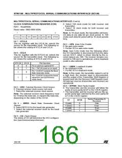
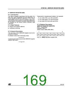
SYNCHRONOUS INPUT CONTROL (SICR)
R254 - Read/Write
Reset value: 0000 0011 (03h)
7
0
DCDE DCDP
Bit 2 = INPEN: All Input Disable.
0: Enable SIN/RXCLK/DCD inputs.
1: Disable SIN/RXCLK/DCD inputs.
SMEN INPL XCKPL
INPEN
X
X
N
L
Bit 7 = SMEN: Synchronous Mode Enable.
0: Disable all features relating to Synchronous
mode (the contents of SICR and SOCR are ig-
nored).
Bit 1:0 = “Don't Care”
167/199
9

 ETC [ ETC ]