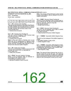
ST90158 - MULTIPROTOCOL SERIAL COMMUNICATIONS INTERFACE (SCI-M)
MULTIPROTOCOL SERIAL COMMUNICATIONS INTERFACE (Cont’d)
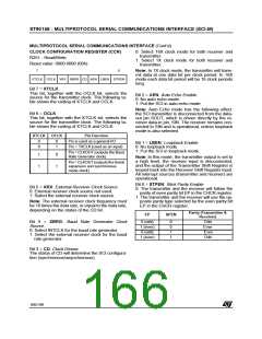
CLOCK CONFIGURATION REGISTER (CCR)
R251 - Read/Write
0: Select 16X clock mode for both receiver and
transmitter.
1: Select 1X clock mode for both receiver and
Reset value: 0000 0000 (00h)
transmitter.
7
0
Note: In 1X clock mode, the transmitter will trans-
mit data at one data bit per clock period. In 16X
mode each data bit period will be 16 clock periods
long.
XTCLK OCLK XRX XBRG CD AEN LBEN STPEN
Bit 7 = XTCLK
This bit, together with the OCLK bit, selects the
source for the transmitter clock. The following ta-
ble shows the coding of XTCLK and OCLK.
Bit 2 = AEN: Auto Echo Enable.
0: No auto echo mode.
1: Put the SCI in auto echo mode.
Note: Auto Echo mode has the following effect:
the SCI transmitter is disconnected from the data-
out pin SOUT, which is driven directly by the re-
ceiver data-in pin, SIN. The receiver remains con-
nected to SIN and is operational, unless loopback
mode is also selected.
Bit 6 = OCLK
This bit, together with the XTCLK bit, selects the
source for the transmitter clock. The following ta-
ble shows the coding of XTCLK and OCLK.
XTCLK
OCLK
Pin Function
0
0
0
1
Pin is used as a general I/O
Pin = TXCLK (used as an input)
Bit 1 = LBEN: Loopback Enable.
0: No loopback mode.
1: Put the SCI in loopback mode.
Pin = CLKOUT (outputs the Baud
Rate Generator clock)
1
0
Note: In this mode, the transmitter output is set to
a high level, the receiver input is disconnected,
and the output of the Transmitter Shift Register is
looped back into the Receiver Shift Register input.
All interrupt sources (transmitter and receiver) are
operational.
Pin = CLKOUT (outputs the Serial
expansion and synchronous
mode clock)
1
1
Bit 0 = STPEN: Stick Parity Enable.
Bit 5 = XRX: External Receiver Clock Source.
0: External receiver clock source not used.
1: Select the external receiver clock source.
0: The transmitter and the receiver will follow the
parity of even parity bit EP in the CHCR register.
1: The transmitter and the receiver will use the op-
posite parity type selected by the even parity bit
EP in the CHCR register.
Note: The external receiver clock frequency must
be 16 times the data rate, or equal to the data rate,
depending on the status of the CD bit.
Parity (Transmitter &
EP
SPEN
Receiver)
Bit 4 = XBRG: Baud Rate Generator Clock
Source.
0: Select INTCLK for the baud rate generator.
1: Select the external receiver clock for the baud
rate generator.
0 (odd)
1 (even)
0 (odd)
0
0
1
1
Odd
Even
Even
1 (even)
Odd
Bit 3 = CD: Clock Divisor.
The status of CD will determine the SCI configura-
tion (synchronous/asynchronous).
166/199
9

 ETC [ ETC ]