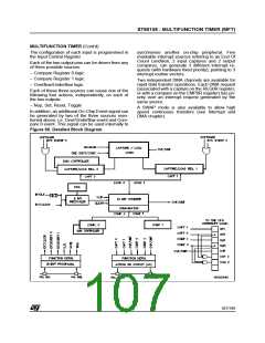
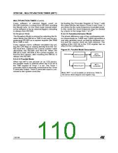
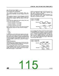
ST90158 - MULTIFUNCTION TIMER (MFT)
MULTIFUNCTION TIMER (Cont’d)
9.3.3 Input Pin Assignment
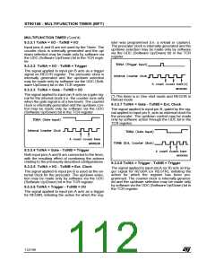
– a trigger signal on the TxINA input pin performs
an U/D counter load if RM0 is reset, or an exter-
nal capture if RM0 is set.
The two external inputs (TxINA and TxINB) of the
timer can be individually configured to catch a par-
ticular external event (i.e. rising edge, falling edge,
or both rising and falling edges) by programming
the two relevant bits (A0, A1 and B0, B1) for each
input in the external Input Control Register
(T_ICR).
– a trigger signal on the TxINB input pin always
performs an external capture on REG1R. The
TxINB input pin is disabled when the Bivalue
Mode is set.
Note: For proper operation of the External Input
The 16 different functional modes of the two exter-
nal inputs can be selected by programming bits
IN0 - IN3 of the T_ICR, as illustrated in Figure 22
pins, the following must be observed:
– the minimum external clock/trigger pulse width
must not be less than the system clock (INTCLK)
period if the input pin is programmed as rising or
falling edge sensitive.
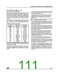
Table 22. Input Pin Function
I C Reg.
IN3-IN0 bits
TxINA Input
Function
TxINB Input
Function
– the minimum external clock/trigger pulse width
must not be less than the prescaler clock period
(INTCLK/3) if the input pin is programmed as ris-
ing and falling edge sensitive (valid also in Auto
discrimination mode).
0000
0001
0010
0011
0100
0101
0110
0111
1000
1001
1010
1011
1100
1101
1110
1111
not used
not used
Gate
Gate
not used
Trigger
not used
Trigger
not used
Trigger
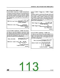
– the minimum delay between two clock/trigger
pulse active edges must be greater than the
prescaler clock period (INTCLK/3), while the
minimum delay between two consecutive clock/
trigger pulses must be greater than the system
clock (INTCLK) period.
Ext. Clock
not used
Ext. Clock
Trigger
Clock Down
Ext. Clock
Trigger Down
not used
Autodiscr.
Ext. Clock
Trigger
Gate
Trigger
Clock Up
Up/Down
Trigger Up
Up/Down
Autodiscr.
Trigger
– the minimum gate pulse width must be at least
twice the prescaler clock period (INTCLK/3).
– in Autodiscrimination mode, the minimum delay
between the input pin A pulse edge and the edge
of the input pin B pulse, must be at least equal to
the system clock (INTCLK) period.
Ext. Clock
Trigger
Gate
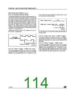
Some choices relating to the external input pin as-
signment are defined in conjunction with the RM0
and RM1 bits in TMR.
– if a number, N, of external pulses must be count-
ed using a Compare Register in External Clock
mode, then the Compare Register must be load-
ed with the value [X +/- (N-1)], where X is the
starting counter value and the sign is chosen de-
pending on whether Up or Down count mode is
selected.
For input pin assignment codes which use the in-
put pins as Trigger Inputs (except for code 1010,
Trigger Up:Trigger Down), the following conditions
apply:
111/199
9

 ETC [ ETC ]