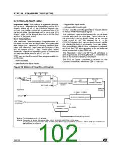
ST90158 - STANDARD TIMER (STIM)
STANDARD TIMER (Cont’d)
9.2.2.4 Standard Timer Output Modes
ic is disabled (i.e. after the DI instruction). It is also
necessary to clear any possible interrupt pending
requests on the corresponding external interrupt
channel before enabling it. A delay instruction (i.e.
a NOP instruction) must be inserted between the
reset of the interrupt pending bit and the INTS
write instruction.
OUTPUT modes are selected using 2 bits of the
STC register: OUTMD1 and OUTMD2.
No Output Mode (OUTMD1 = “0”, OUTMD2 = “0”)
The output is disabled and the corresponding pin
is set high, in order to allow other alternate func-
tions to use the I/O pin.
Square Wave Output Mode (OUTMD1 = “0”,
OUTMD2 = “1”)
9.2.4 Register Mapping
Depending on the ST9 device there may be up to 4
Standard Timers (refer to the block diagram in the
first section of the data sheet).
The Standard Timer toggles the state of the
STOUT pin on every End Of Count condition. With
INTCLK = 24MHz, this allows generation of a
square wave with a period ranging from 333ns to
5.59 seconds.
Each Standard Timer has 4 registers mapped into
Page 11 in Group F of the Register File
In the register description on the following page,
register addresses refer to STIM0 only.
PWM Output Mode (OUTMD1 = “1”)
The value of the OUTMD2 bit is transferred to the
STOUT output pin at the End Of Count. This al-
lows the user to generate PWM signals, by modi-
fying the status of OUTMD2 between End of Count
events, based on software counters decremented
on the Standard Timer interrupt.
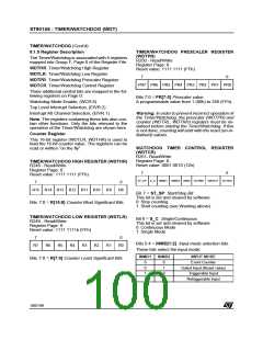
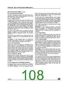
STD Timer Register
Register Address
R240 (F0h)
STIM0
STIM1
STIM2
STIM3
STH0
STL0
STP0
STC0
STH1
STL1
STP1
STC1
STH2
STL2
STP2
STC2
STH3
STL3
STP3
STC3
R241 (F1h)
R242 (F2h)
R243 (F3h)
R244 (F4h)
R245 (F5h)
R246 (F6h)
R247 (F7h)
R248 (F8h)
R249 (F9h)
R250 (FAh)
R251 (FBh)
R252 (FCh)
R253 (FDh)
R254 (FEh)
R255 (FFh)
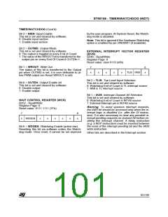
9.2.3 Interrupt Selection
The Standard Timer may generate an interrupt re-
quest at every End of Count.
Bit 2 of the STC register (INTS) selects the inter-
rupt source between the Standard Timer interrupt
and the external interrupt pin. Thus the Standard
Timer Interrupt uses the interrupt channel and
takes the priority and vector of the external inter-
rupt channel.
If INTS is set to “1”, the Standard Timer interrupt is
disabled; otherwise, an interrupt request is gener-
ated at every End of Count.
Note: When enabling or disabling the Standard
Timer Interrupt (writing INTS in the STC register)
an edge may be generated on the interrupt chan-
nel, causing an unwanted interrupt.
Note: The four standard timers are not implement-
ed on all ST9 devices. Refer to the block diagram
of the device for the number of timers.
To avoid this spurious interrupt request, the INTS
bit should be accessed only when the interrupt log-
104/199
9

 ETC [ ETC ]