ST72104G, ST72215G, ST72216G, ST72254G
16-BIT TIMER (Cont’d)
CONTROL REGISTER 2 (CR2)
Read/Write
Bit 4 = PWM Pulse Width Modulation.
0: PWM mode is not active.
1: PWM mode is active, the OCMP1 pin outputs a
programmable cyclic signal; the length of the
pulse depends on the value of OC1R register;
the period depends on the value of OC2R regis-
ter.
Reset Value: 0000 0000 (00h)
7
0
OC1E OC2E OPM PWM CC1 CC0 IEDG2 EXEDG
Bits 3:2 = CC[1:0] Clock Control.
Bit 7 = OC1E Output Compare 1 Pin Enable.
This bit is used only to output the signal from the
timer on the OCMP1 pin (OLV1 in Output Com-
pare mode, both OLV1 and OLV2 in PWM and
one-pulse mode). Whatever the value of the OC1E
bit, the internal Output Compare 1 function of the
timer remains active.
0: OCMP1 pin alternate function disabled (I/O pin
free for general-purpose I/O).
1: OCMP1 pin alternate function enabled.
The timer clock mode depends on these bits:
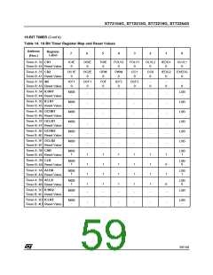
Table 13. Clock Control Bits
Timer Clock
fCPU / 4
CC1
CC0
0
0
1
0
1
0
fCPU / 2
fCPU / 8
External Clock (where
available)
1
1
Bit 6 = OC2E Output Compare 2 Pin Enable.
This bit is used only to output the signal from the
timer on the OCMP2 pin (OLV2 in Output Com-
pare mode). Whatever the value of the OC2E bit,
the internal Output Compare 2 function of the timer
remains active.
0: OCMP2 pin alternate function disabled (I/O pin
free for general-purpose I/O).
1: OCMP2 pin alternate function enabled.
Note: If the external clock pin is not available, pro-
gramming the external clock configuration stops
the counter.
Bit 1 = IEDG2 Input Edge 2.
This bit determines which type of level transition
on the ICAP2 pin will trigger the capture.
0: A falling edge triggers the capture.
1: A rising edge triggers the capture.
Bit 5 = OPM One Pulse mode.
0: One Pulse mode is not active.
Bit 0 = EXEDG External Clock Edge.
1: One Pulse mode is active, the ICAP1 pin can be
used to trigger one pulse on the OCMP1 pin; the
active transition is given by the IEDG1 bit. The
length of the generated pulse depends on the
contents of the OC1R register.
This bit determines which type of level transition
on the external clock pin (EXTCLK) will trigger the
counter register.
0: A falling edge triggers the counter register.
1: A rising edge triggers the counter register.
56/140

 ETC [ ETC ]