ST72104G, ST72215G, ST72216G, ST72254G
16-BIT TIMER (Cont’d)
12.2.7 Register Description
Bit 4 = FOLV2 Forced Output Compare 2.
This bit is set and cleared by software.
0: No effect on the OCMP2 pin.
1:Forces the OLVL2 bit to be copied to the
OCMP2 pin, if the OC2E bit is set and even if
there is no successful comparison.
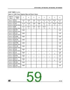
Each Timer is associated with three control and
status registers, and with six pairs of data registers
(16-bit values) relating to the two input captures,
the two output compares, the counter and the al-
ternate counter.
Bit 3 = FOLV1 Forced Output Compare 1.
This bit is set and cleared by software.
0: No effect on the OCMP1 pin.
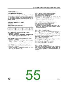
CONTROL REGISTER 1 (CR1)
Read/Write
1: Forces OLVL1 to be copied to the OCMP1 pin, if
the OC1E bit is set and even if there is no suc-
cessful comparison.
Reset Value: 0000 0000 (00h)
7
0
ICIE OCIE TOIE FOLV2 FOLV1 OLVL2 IEDG1 OLVL1
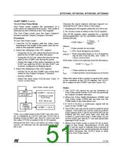
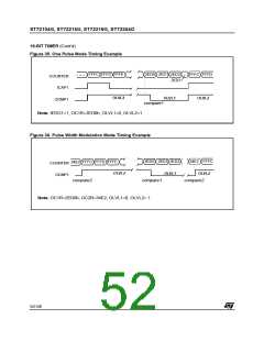
Bit 2 = OLVL2 Output Level 2.
This bit is copied to the OCMP2 pin whenever a
successful comparison occurs with the OC2R reg-
ister and OCxE is set in the CR2 register. This val-
ue is copied to the OCMP1 pin in One Pulse mode
and Pulse Width Modulation mode.
Bit 7 = ICIE Input Capture Interrupt Enable.
0: Interrupt is inhibited.
1: A timer interrupt is generated whenever the
ICF1 or ICF2 bit of the SR register is set.
Bit 1 = IEDG1 Input Edge 1.
Bit 6 = OCIE Output Compare Interrupt Enable.
0: Interrupt is inhibited.
1: A timer interrupt is generated whenever the
OCF1 or OCF2 bit of the SR register is set.
This bit determines which type of level transition
on the ICAP1 pin will trigger the capture.
0: A falling edge triggers the capture.
1: A rising edge triggers the capture.
Bit 5 = TOIE Timer Overflow Interrupt Enable.
0: Interrupt is inhibited.
1: A timer interrupt is enabled whenever the TOF
bit of the SR register is set.
Bit 0 = OLVL1 Output Level 1.
The OLVL1 bit is copied to the OCMP1 pin when-
ever a successful comparison occurs with the
OC1R register and the OC1E bit is set in the CR2
register.
55/140

 ETC [ ETC ]