ST72104G, ST72215G, ST72216G, ST72254G
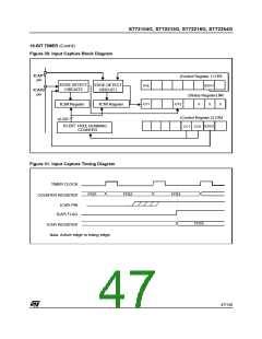
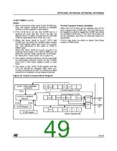
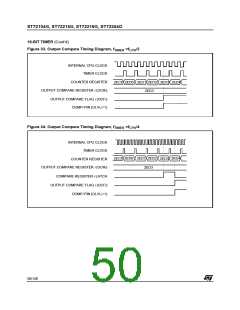
16-BIT TIMER (Cont’d)
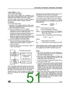
12.2.3.5 One Pulse Mode
Clearing the Input Capture interrupt request (i.e.
clearing the ICFi bit) is done in two steps:
One Pulse mode enables the generation of a
pulse when an external event occurs. This mode is
selected via the OPM bit in the CR2 register.
1. Reading the SR register while the ICFi bit is set.
2. An access (read or write) to the ICiLR register.
The One Pulse mode uses the Input Capture1
function and the Output Compare1 function.
The OC1R register value required for a specific
timing application can be calculated using the fol-
lowing formula:
Procedure:
t * f
To use One Pulse mode:
CPU
- 5
OCiR Value =
1. Load the OC1R register with the value corre-
sponding to the length of the pulse (see the for-
mula in the opposite column).
PRESC
Where:
t
= Pulse period (in seconds)
2. Select the following in the CR1 register:
f
= CPU clock frequency (in hertz)
CPU
PRESC
– Using the OLVL1 bit, select the level to be ap-
plied to the OCMP1 pin after the pulse.
= Timer prescaler factor (2, 4 or 8 depend-
ing on the CC[1:0] bits, see Table 13
Clock Control Bits)
– Using the OLVL2 bit, select the level to be ap-
plied to the OCMP1 pin during the pulse.
If the timer clock is an external clock the formula is:
– Select the edge of the active transition on the
ICAP1 pin with the IEDG1 bit (the ICAP1 pin
must be configured as floating input).
OCiR = t f
-5
* EXT
Where:
t
3. Select the following in the CR2 register:
= Pulse period (in seconds)
– Set the OC1E bit, the OCMP1 pin is then ded-
icated to the Output Compare 1 function.
f
= External timer clock frequency (in hertz)
EXT
– Set the OPM bit.
When the value of the counter is equal to the value
of the contents of the OC1R register, the OLVL1
bit is output on the OCMP1 pin (see Figure 35).
– Select the timer clock CC[1:0] (see Table 13
Clock Control Bits).
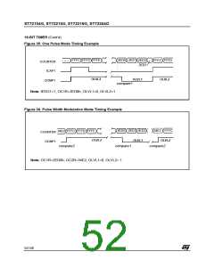
One Pulse mode cycle
Notes:
1. The OCF1 bit cannot be set by hardware in
One Pulse mode but the OCF2 bit can generate
an Output Compare interrupt.
When
OCMP1 = OLVL2
event occurs
on ICAP1
Counter is reset
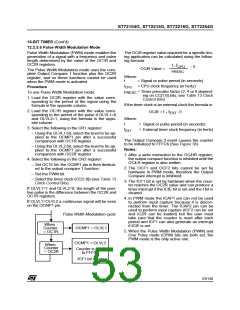
2. When the Pulse Width Modulation (PWM) and
One Pulse mode (OPM) bits are both set, the
PWM mode is the only active one.
to FFFCh
ICF1 bit is set
3. If OLVL1=OLVL2 a continuous signal will be
seen on the OCMP1 pin.
When
Counter
OCMP1 = OLVL1
= OC1R
4. The ICAP1 pin can not be used to perform input
capture. The ICAP2 pin can be used to perform
input capture (ICF2 can be set and IC2R can be
loaded) but the user must take care that the
counter is reset each time a valid edge occurs
on the ICAP1 pin and ICF1 can also generates
interrupt if ICIE is set.
Then, on a valid event on the ICAP1 pin, the coun-
ter is initialized to FFFCh and the OLVL2 bit is
loaded on the OCMP1 pin, the ICF1 bit is set and
the value FFFDh is loaded in the IC1R register.
Because the ICF1 bit is set when an active edge
occurs, an interrupt can be generated if the ICIE
bit is set.
5. When One Pulse mode is used OC1R is dedi-
cated to this mode. Nevertheless OC2R and
OCF2 can be used to indicate that a period of
time has elapsed but cannot generate an output
waveform because the OLVL2 level is dedi-
cated to One Pulse mode.
51/140

 ETC [ ETC ]