ST72104G, ST72215G, ST72216G, ST72254G
Forced Compare Output capability
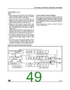
16-BIT TIMER (Cont’d)
Notes:
1. After a processor write cycle to the OCiHR reg-
ister, the output compare function is inhibited
until the OCiLR register is also written.
When the FOLVi bit is set by software, the OLVLi
bit is copied to the OCMPi pin. The OLVi bit has to
be toggled in order to toggle the OCMPi pin when
it is enabled (OCiE bit=1). The OCFi bit is then not
set by hardware, and thus no interrupt request is
generated.
2. If the OCiE bit is not set, the OCMPi pin is a
general I/O port and the OLVLi bit will not
appear when a match is found but an interrupt
could be generated if the OCIE bit is set.
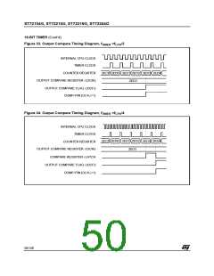
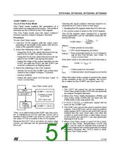
3. When the timer clock is f
/2, OCFi and
FOLVLi bits have no effect in either One-Pulse
CPU
OCMPi are set while the counter value equals
the OCiR register value (see Figure 33 on page
53). This behaviour is the same in OPM or
PWM mode.
mode or PWM mode.
When the timer clock is f
/4, f
/8 or in
CPU
CPU
external clock mode, OCFi and OCMPi are set
while the counter value equals the OCiR regis-
ter value plus 1 (see Figure 34 on page 53).
4. The output compare functions can be used both
for generating external events on the OCMPi
pins even if the input capture mode is also
used.
5. The value in the 16-bit OCiR register and the
OLVi bit should be changed after each suc-
cessful comparison in order to control an output
waveform or establish a new elapsed timeout.
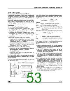
Figure 32. Output Compare Block Diagram
16 BIT FREE RUNNING
OC1E
CC1 CC0
OC2E
COUNTER
(Control Register 2) CR2
16-bit
(Control Register 1) CR1
OUTPUT COMPARE
CIRCUIT
Latch
1
FOLV2 FOLV1
OCIE
OLVL2
OLVL1
OCMP1
Pin
16-bit
16-bit
Latch
2
OCMP2
Pin
OC1R Register
OCF1
OCF2
0
0
0
OC2R Register
(Status Register) SR
49/140

 ETC [ ETC ]