ST72104G, ST72215G, ST72216G, ST72254G
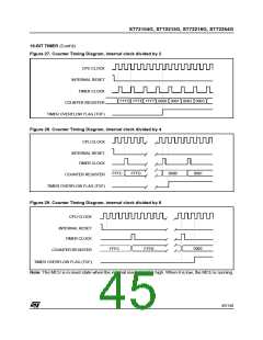
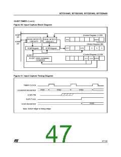
16-BIT TIMER (Cont’d)
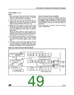
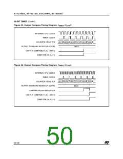
12.2.3.4 Output Compare
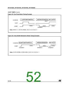
– The OCMPi pin takes OLVLi bit value (OCMPi
pin latch is forced low during reset).
In this section, the index, i, may be 1 or 2 because
there are 2 output compare functions in the 16-bit
timer.
– A timer interrupt is generated if the OCIE bit is
set in the CR2 register and the I bit is cleared in
the CC register (CC).
This function can be used to control an output
waveform or indicate when a period of time has
elapsed.
The OCiR register value required for a specific tim-
ing application can be calculated using the follow-
ing formula:
When a match is found between the Output Com-
pare register and the free running counter, the out-
put compare function:
– Assigns pins with a programmable value if the
OCIE bit is set
∆t f
* CPU
PRESC
∆ OCiR =
– Sets a flag in the status register
– Generates an interrupt if enabled
Where:
∆t
= Output compare period (in seconds)
= CPU clock frequency (in hertz)
Two 16-bit registers Output Compare Register 1
(OC1R) and Output Compare Register 2 (OC2R)
contain the value to be compared to the counter
register each timer clock cycle.
f
CPU
PRESC
= Timer prescaler factor (2, 4 or 8 de-
pending on CC[1:0] bits, see Table 13
Clock Control Bits)
MS Byte
OCiHR
LS Byte
OCiLR
OCiR
If the timer clock is an external clock, the formula
is:
These registers are readable and writable and are
not affected by the timer hardware. A reset event
changes the OCiR value to 8000h.
∆ OCiR = ∆t f
* EXT
Timing resolution is one count of the free running
Where:
counter: (f
).
CC[1:0]
CPU/
∆t
= Output compare period (in seconds)
= External timer clock frequency (in hertz)
f
EXT
Procedure:
To use the output compare function, select the fol-
lowing in the CR2 register:
Clearing the output compare interrupt request (i.e.
clearing the OCFi bit) is done by:
– Set the OCiE bit if an output is needed then the
OCMPi pin is dedicated to the output compare i
signal.
1. Reading the SR register while the OCFi bit is
set.
2. An access (read or write) to the OCiLR register.
– Select the timer clock (CC[1:0]) (see Table 13
Clock Control Bits).
The following procedure is recommended to pre-
vent the OCFi bit from being set between the time
it is read and the write to the OCiR register:
And select the following in the CR1 register:
– Select the OLVLi bit to applied to the OCMPi pins
after the match occurs.
– Write to the OCiHR register (further compares
are inhibited).
– Set the OCIE bit to generate an interrupt if it is
needed.
– Read the SR register (first step of the clearance
of the OCFi bit, which may be already set).
When a match is found between OCRi register
and CR register:
– Write to the OCiLR register (enables the output
compare function and clears the OCFi bit).
– OCFi bit is set.
48/140

 ETC [ ETC ]