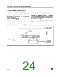
ST72104G, ST72215G, ST72216G, ST72254G
RESET SEQUENCE MANAGER (Cont’d)
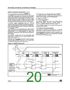
7.2.2 Asynchronous External RESET pin
7.2.3 Internal Low Voltage Detection RESET
The RESET pin is both an input and an open-drain
Two different RESET sequences caused by the in-
ternal LVD circuitry can be distinguished:
output with integrated R
weak pull-up resistor.
ON
This pull-up has no fixed value but varies in ac-
cordance with the input voltage. It can be pulled
low by external circuitry to reset the device. See
electrical characteristics section for more details.
■ Power-On RESET
■ Voltage Drop RESET
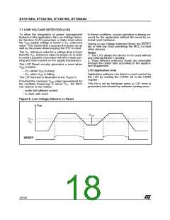
The device RESET pin acts as an output that is
pulled low when V <V
(rising edge) or
DD
IT+
A RESET signal originating from an external
V
<V (falling edge) as shown in Figure 12.
DD
IT-
source must have a duration of at least t
in
h(RSTL)in
The LVD filters spikes on V larger than t
avoid parasitic resets.
to
g(VDD)
order to be recognized. This detection is asynchro-
nous and therefore the MCU can enter reset state
even in HALT mode.
DD
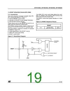
7.2.4 Internal Watchdog RESET
The RESET pin is an asynchronous signal which
plays a major role in EMS performance. In a noisy
environment, it is recommended to follow the
guidelines mentioned in the electrical characteris-
tics section.
The RESET sequence generated by a internal
Watchdog counter overflow is shown in Figure 12.
Starting from the Watchdog counter underflow, the
device RESET pin acts as an output that is pulled
low during at least t
.
w(RSTL)out
Two RESET sequences can be associated with
this RESET source: short or long external reset
pulse (see Figure 12).
Starting from the external RESET pulse recogni-
tion, the device RESET pin acts as an output that
is pulled low during at least t
.
w(RSTL)out
Figure 12. RESET Sequences
V
DD
V
V
IT+
IT-
LVD
RESET
SHORT EXT.
RESET
LONG EXT.
RESET
WATCHDOG
RESET
RUN
RUN
RUN
RUN
RUN
DELAY
DELAY
DELAY
DELAY
t
t
w(RSTL)out
h(RSTL)in
t
w(RSTL)out
t
h(RSTL)in
EXTERNAL
RESET
SOURCE
RESET PIN
WATCHDOG
RESET
WATCHDOG UNDERFLOW
INTERNAL RESET (4096 TCPU
FETCH VECTOR
)
20/140

 ETC [ ETC ]