ST72104G, ST72215G, ST72216G, ST72254G
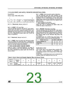
7.2 RESET SEQUENCE MANAGER (RSM)
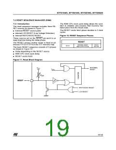
7.2.1 Introduction
The 4096 CPU clock cycle delay allows the oscil-
lator to stabilise and ensures that recovery has
taken place from the Reset state.
The reset sequence manager includes three RE-
SET sources as shown in Figure 11:
The RESET vector fetch phase duration is 2 clock
cycles.
■ External RESET source pulse
■ Internal LVD RESET (Low Voltage Detection)
■ Internal WATCHDOG RESET
Figure 10. RESET Sequence Phases
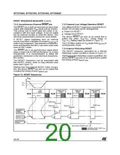
These sources act on the RESET pin and it is al-
ways kept low during the delay phase.
RESET
The RESET service routine vector is fixed at ad-
dresses FFFEh-FFFFh in the ST7 memory map.
INTERNAL RESET
FETCH
DELAY
4096 CLOCK CYCLES
VECTOR
The basic RESET sequence consists of 3 phases
as shown in Figure 10:
■ Delay depending on the RESET source
■ 4096 CPU clock cycle delay
■ RESET vector fetch
Figure 11. Reset Block Diagram
INTERNAL
RESET
V
DD
f
CPU
R
ON
RESET
WATCHDOG RESET
LVD RESET
19/140

 ETC [ ETC ]