ST6200C/ST6201C/ST6203C
8-BIT ADC CHARACTERISTICS (Cont’d)
ADC Accuracy
Symbol
Parameter
Conditions
Min
Typ.
Max
Unit
±2, fosc>1.2MHz
±4, fosc>32KHz
1)
1.2
|E |
Total unadjusted error
T
1)
0.72
-0.31
0.54
E
Offset error
2)
O
V
=5V
DD
LSB
1)
E
Gain Error
f
=8MHz
G
OSC
1)
|E |
Differential linearity error
D
1)
|E |
Integral linearity error
L
Notes:
1. Negative injection disturbs the analog performance of the device. In particular, it induces leakage currents throughout
the device including the analog inputs. To avoid undesirable effects on the analog functions, care must be taken:
- Analog input pins must have a negative injection less than 1mA (assuming that the impedance of the analog voltage
is lower than the specified limits).
- Pure digital pins must have a negative injection less than 1mA. In addition, it is recommended to inject the current as
far as possible from the analog input pins.
2. Data based on characterization results over the whole temperature range, monitored in production.
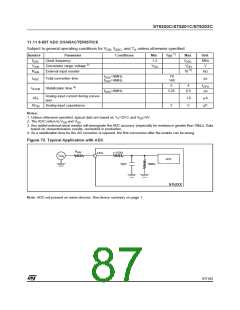
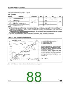
Figure 73. ADC Accuracy Characteristics
Digital Result ADCDR
E
G
(1) Example of an actual transfer curve
(2) The ideal transfer curve
(3) End point correlation line
255
254
253
V
– V
DDA
SSA
1LSB
= ----------------------------------------
IDE AL
256
(2)
E =Total Unadjusted Error: maximum deviation
T
E
between the actual and the ideal transfer curves.
T
(3)
7
6
5
4
3
2
1
E =Offset Error: deviation between the first actual
O
(1)
transition and the first ideal one.
E =Gain Error: deviation between the last ideal
G
transition and the last actual one.
E
O
E
L
E =Differential Linearity Error: maximum deviation
D
between actual steps and the ideal one.
E =Integral Linearity Error: maximum deviation
L
E
between any actual transition and the end point
correlation line.
D
1 LSB
IDEAL
7
V
(LSB
)
in
IDEAL
0
1
2
3
4
5
6
253 254 255 256
V
V
DDA
SSA
Note: ADC not present on some devices. See device summary on page 1.
88/104
1

 ETC [ ETC ]