ST6200C/ST6201C/ST6203C
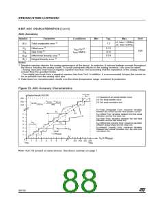
11.11 8-BIT ADC CHARACTERISTICS
Subject to general operating conditions for V , f
, and T unless otherwise specified.
DD OSC
A
1)
Symbol
Parameter
Clock frequency
Conditions
Min
Typ
Max
Unit
MHz
V
f
1.2
f
OSC
OSC
2)
V
Conversion range voltage
External input resistor
V
V
AIN
SS
DD
3)
R
10
kΩ
AIN
f
=8MHz
=4MHz
70
140
OSC
t
Total convertion time
µs
ADC
f
OSC
2
4
t
CPU
4)
t
Stabilization time
STAB
f
=8MHz
3.25
6.5
1.0
5
µs
µA
pF
OSC
Analog input current during conver-
sion
AD
I
AC
Analog input capacitance
2
IN
Notes:
1. Unless otherwise specified, typical data are based on T =25°C and V =5V.
A
DD
2. The ADC refers to V and V
.
DD
SS
3. Any added external serial resistor will downgrade the ADC accuracy (especially for resistance greater than 10kΩ). Data
based on characterization results, not tested in production.
4. As a stabilization time for the AD converter is required, the first conversion after the enable can be wrong.
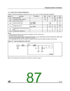
Figure 72. Typical Application with ADC
R
AIN
r≈150Ω
AINx
V
AIN
ADC
10pF
10MΩ
ST62XX
Note: ADC not present on some devices. See device summary on page 1.
87/104
1

 ETC [ ETC ]