RTL8211C & RTL8211CL
Datasheet
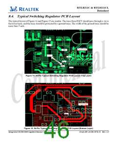
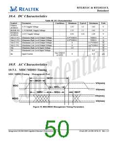
8.4. Typical Switching Regulator PCB Layout
The typical layout of Figure 14 and Figure 15 are similar. The trace from RSET should pass through a via to
the lower layer, and the trace should be protected by a ground trace. The width of the ground trace should be
more than 5 mils.
Figure 14. 64-Pin Typical Switching Regulator PCB Layout (Top Layer)
Figure 15. 64-Pin Typical Switching Regulator PCB Layout (Bottom Layer)
Integrated 10/100/1000 Gigabit Ethernet Transceiver 40 Track ID: JATR-1076-21 Rev. 1.3

 ETC [ ETC ]