RTL8211C & RTL8211CL
Datasheet
10. Characteristics
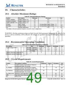
10.1. Absolute Maximum Ratings
Table 42. Absolute Maximum Ratings
Minimum
Symbol
Description
Maximum
Unit
V
VDD33, AVDD33
AVDD10, DVDD10
Supply Voltage 3.3V
Supply Voltage 1.05V
-0.4
-0.1
-0.2
-0.5
-0.3
-55
+0.4
+0.1
V
VDD25 (RGMII 2.5V) Supply Voltage 2.5V
+0.3
V
DCinput
DCoutput
NA
Input Voltage
Corresponding Supply Voltage + 0.5
Corresponding Supply Voltage + 0.5
+125
V
Output Voltage
Storage Temperature
V
°C
Note:Refer to the most updated schematic circuit for correct configuration.
WARNING: Absolute maximum ratings are limits beyond which permanent damage may be caused to the
device, or device reliability will be affected. All voltages are specified reference to GND unless otherwise
specified.
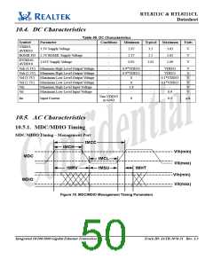
10.2. Recommended Operating Conditions
Table 43. Recommended Operating Conditions
Description
Pins
Minimum
Typical
Maximum
3.63
Unit
V
Supply Voltage VDD
DVDD33, AVDD33
2.97
0.95
2.37
0
3.3
1.05
2.5
-
AVDD10, DVDD10
1.09
V
2.5V RGMII
2.62
V
Ambient Operating Temperature TA
Maximum Junction Temperature
-
-
70
°C
°C
-
-
125
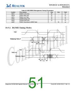
10.3. Crystal Requirements
Table 44. Crystal Requirements
Minimum Typical
Symbol
Description/Condition
Maximum
Unit
Fref
Parallel resonant crystal reference frequency,
fundamental mode, AT-cut type.
-
25
-
MHz
Fref Stability
Parallel resonant crystal frequency stability,
fundamental mode, AT-cut type. Ta=0°C~70°C.
Parallel resonant crystal frequency tolerance,
-30
-50
-
+30
+50
ppm
ppm
Fref Tolerance
-
fundamental mode, AT-cut type. Ta=25°C.
Fref Duty Cycle Reference clock input duty cycle.
40
-
-
-
-
60
30
%
Ω
ESR
DL
Equivalent Series Resistance.
Drive Level.
-
0.5
mW
Integrated 10/100/1000 Gigabit Ethernet Transceiver
43
Track ID: JATR-1076-21 Rev. 1.3

 ETC [ ETC ]