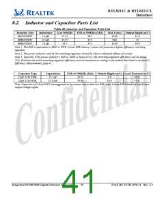
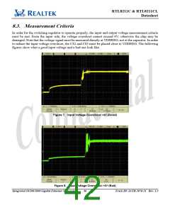
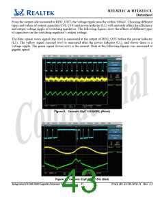
RTL8211C & RTL8211CL
Datasheet
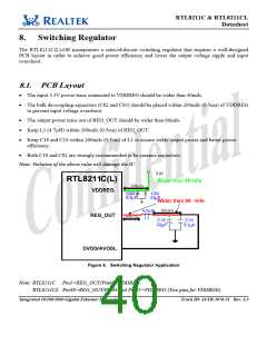
8. Switching Regulator
The RTL8211C(L)-GR incorporates a state-of-the-art switching regulator that requires a well-designed
PCB layout in order to achieve good power efficiency and lower the output voltage ripple and input
overshoot.
8.1. PCB Layout
• The input 3.3V power trace connected to VDDREG should be wider than 40mils.
• The bulk de-coupling capacitors (C82 and C83) should be placed within 200mils (0.5cm) of VDDREG
to prevent input voltage overshoot.
• The output power trace out of REG_OUT should be wider than 60mils.
• Keep L1 (4.7µH) within 200mils (0.5cm) of REG_OUT.
• Keep C18 and C19 within 200mils (0.5cm) of L1 to ensure stable output power and better power
efficiency.
• Both C18 and C82 are strongly recommended to be ceramic capacitors.
Note: Violation of the above rules will damage the IC.
Figure 6. Switching Regulator Application
Note: RTL8211C Pin1=REG_OUT/Pin63=VDDREG
RTL8211CL Pin48=REG_OUT/Pin44 and Pin45=VDDREG (Two pins for VDDRGE)
Integrated 10/100/1000 Gigabit Ethernet Transceiver
34
Track ID: JATR-1076-21 Rev. 1.3

 ETC [ ETC ]