IP1001 LF
Data Sheet
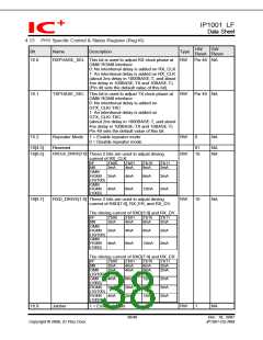
4.13 PHY Specific Control & Status Register (Reg16)
HW
Reset Reset
SW
Bit
Name
Description
Type
16.0
RXPHASE_SEL This bit is used to adjust RX clock phase at RW
GMII/ RGMII interface
Pin 48 NA
0: No intentional delay is added on RX_CLK
1: An intentional delay is added on RX_CLK
(about 2ns delay in 1000BASE-T, and about
4ns delay in 100BASE-TX and 10BASE-T).
(Pin 48 sets the default value of this bit)
16.1
TXPHASE_SEL This bit is used to adjust TX clock phase at
GMII/ RGMII interface
RW
Pin 49 NA
0: No intentional delay is added on
GTX_CLK/ TXC
1: An intentional delay is added on
GTX_CLK/ TXC
(about 2ns delay in 1000BASE-T, and about
4ns delay in 100BASE-TX and 10BASE-T)
Pin 49 sets the default value of this bit.
16.2
Repeater Mode 1 = Enable repeater mode
0 = Disable repeater mode
RW
RW
0
NA
16[4:3]
16[6:5]
Reserved
01
10
NA
NA
RXCLK_DRIVE[1:0]
These 2 bits are used to adjust driving
current of RX_CLK.
I/F
2’b00
2’b01
2’b10
2’b11
MII
2mA
4mA
8mA
2mA
GMII/
RGMII
(10/100)
GMII/
RGMII
(1000)
2mA
4mA
4mA
8mA
8mA
2mA
2mA
12mA
16[8:7]
RXD_DRIVE[1:0] These 2 bits are used to adjust driving
current of RXD[7:0], RX_ER, and RX_DV.
RW
10
NA
The driving current of RXD[3:0] and RX_DV
I/F
2’b00
2’b01
2’b10
2’b11
MII
2mA
4mA
8mA
2mA
GMII/
RGMII
(10/100)
GMII/
RGMII
(1000)
2mA
4mA
4mA
8mA
8mA
2mA
2mA
12mA
The driving current of RXD[7:4] and RX_ER
I/F
MII
GMII
2’b00
2mA
2mA
2’b01
4mA
4mA
2’b10
8mA
8mA
2’b11
2mA
2mA
(10/100)
GMII
4mA
2mA
4mA
8mA
2mA
2mA
12mA
2mA
2mA
2mA
2mA
(1000)
RGMII
(10/100)
RGMII
(1000)
12mA
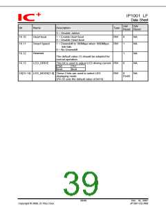
16.9
Jabber
1 = Enable Jabber
RW
1
NA
38/48
Dec. 18, 2007
IP1001-DS-R06
Copyright © 2006, IC Plus Corp.

 ETC [ ETC ]