IP1001 LF
Data Sheet
3.2
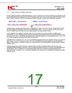
MAC Interface (RGMII/ GMII/ MII)
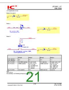
IP1001 supports RGMII and GMII/ MII interfaces. User can select the one of the interfaces by configure pin 36
and IP1001 will latch the setting at the end of hardware reset. If pin 36 is connected to GND through a resistor
R44, RGMII is selected. If pin 36 is connected to VDDO through a resistor R24, GMII/ MII is selected.
GMII/MII interface
RGMII interface
VDDO
RGMII_N/GMII
R24 5.1K
R44 5.1K RGMII_N/GMII
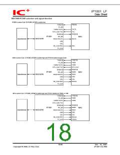
If GMII mode is selected and IP1001 links in 1000BASE-T mode, GTX_CLK, TX_EN, TXD[7:0] and TX_ER
are input signals and should be driven by an external MAC device, TX_CLK is driven low. RX_CLK, CRS,
RX_DV, RXD[7:0], RX_ER and COL are output signals to an external MAC device.
In the 100BASE-TX (10BASE-T) modes, both TX_CLK and RX_CLK source 25 MHz (2.5 MHz) clock
respectively. TX_EN, TXD[3:0] and TX_ER are input signal and should be driven by an external MAC device.
RX_CLK, CRS, RX_DV, RXD[3:0], RX_ER and COL are output signals to an external MAC device. GTX_CLK
and TXD[7:4] signals are ignored and RXD[7:4] drives low.
If RGMII mode is selected, TXC, TX_CTL and TXD[3:0] are input signals and should be driven by an external
MAC device, TX_CLK is driven low. RXC, RX_CTL and RXD[3:0] are output signals to an external MAC
device. RXC provides a 125 Mhz, 25 Mhz or 2.5 Mhz reference clock depending on the link speed is 1000M,
100M or 10M.
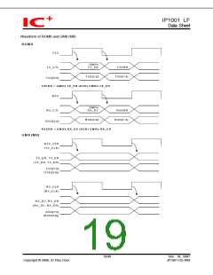
A timing adjustment on MAC interface is implemented in IP1001 by adding delay to the clock pins and
changing driving capability on RX pins. User can add input delay to the GTX_CLK(TXC) by programming pin
49 TXPHASE_SEL or register 16.1 or add output delay to the RX_CLK(RXC) by programming pin 48
RXPHASE_SEL or register 16.0. The driving capability of RX signals can be configured by programming MII
register 16[8:5]
17/48
Dec. 18, 2007
IP1001-DS-R06
Copyright © 2006, IC Plus Corp.

 ETC [ ETC ]