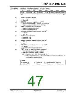
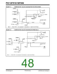
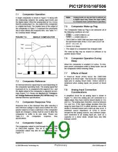
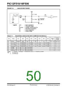
PIC12F510/16F506
8.2
Voltage Reference Accuracy/Error
8.0
COMPARATOR VOLTAGE
REFERENCE MODULE
(PIC16F506 ONLY)
The full range of VSS to VDD cannot be realized due to
construction of the module. The transistors on the top
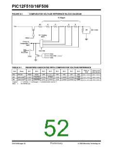
and bottom of the resistor ladder network (Figure 8-1)
keep CVREF from approaching VSS or VDD. The excep-
tion is when the module is disabled by clearing the
VREN bit (VRCON<7>). When disabled, the reference
voltage is VSS when VR<3:0> is ‘0000’ and the VRR
(VRCON<5>) bit is set. This allows the comparator to
detect a zero-crossing and not consume the CVREF
module current.
The Comparator Voltage Reference module also
allows the selection of an internally generated voltage
reference for one of the C2 comparator inputs. The
VRCON register (Register 8-1) controls the Voltage
Reference module shown in Figure 8-1.
8.1
Configuring The Voltage
Reference
The voltage reference is VDD derived and, therefore,
the CVREF output changes with fluctuations in VDD. The
tested absolute accuracy of the comparator voltage ref-
erence can be found in Section 13.2 “DC Character-
istics: PIC12F510/16F506 (Extended)”.
The voltage reference can output 32 voltage levels; 16
in a high range and 16 in a low range.
Equation 8-1 determines the output voltages:
EQUATION 8-1:
VRR = 1 (low range): CVREF = (VR3:VR0/24) x VDD
VRR = 0 (high range):
CVREF = (VDD/4) + (VR3:VR0 x VDD/32)
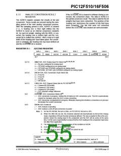
REGISTER 8-1:
VRCON: PIC16F506 ONLY (ADDRESS: 0Ch)
R/W-0
VREN
R/W-0
VROE
R/W-1
VRR
U-0
—
R/W-1
VR3
R/W-1
VR2
R/W-1
VR1
R/W-1
VR0
bit 7
bit 0
bit 7
bit 6
bit 5
VREN: CVREF Enable bit
1= CVREF is powered on
0= CVREF is powered down, no current is drawn
VROE: CVREF Output Enable bit(1)
1= VREF output is enabled
0= VREF output is disabled
VRR: CVREF Range Selection bit
1= Low range
0= High range
bit 4
Unimplemented: Read as ‘0’
bit 3-0
VR<3:0> CVREF Value Selection bit
When VRR = 1: CVREF= (VR<3:0>/24)*VDD
When VRR = 0: CVREF= VDD/4+(VR<3:0>/32)*VDD
Note 1: When this bit is set, the TRIS for the VREF pin is overridden and the analog voltage
is placed on the VREF pin.
2: VREF controls for ratio metric reference applies to Comparator 2 on the PIC12F506
only.
Legend:
R = Readable bit
-n = Value at POR
W = Writable bit
‘1’ = Bit is set
U = Unimplemented bit, read as ‘0’
‘0’ = Bit is cleared x = Bit is unknown
© 2006 Microchip Technology Inc.
Preliminary
DS41268B-page 49

 ETC [ ETC ]