PIC12F510/16F506
9.0
ANALOG-TO-DIGITAL (A/D)
CONVERTER
Note:
It is the users responsibility to ensure that
use of the ADC and comparator simulta-
neously on the same pin, does not
adversely affect the signal being
monitored or adversely effect device
operation.
The A/D Converter allows conversion of an analog
signal into an 8-bit digital signal.
9.1
Clock Divisors
The ADC has 4 clock source settings ADCS<1:0>.
There are 3 divisor values 32, 16 and 8. The fourth set-
ting is INTOSC with a divisor of 4. These settings will
allow a proper conversion when using an external
oscillator at speeds from 20 MHz to 350 kHz. Using an
external oscillator at a frequency below 350 kHz
requires the ADC oscillator setting to be INTOSC/8 for
valid ADC results.
When the CHS<1:0> bits are changed during an ADC
conversion, the new channel will not be selected until
the current conversion is completed. This allows the
current conversion to complete with valid results. All
channel selection information will be lost when the
device enters Sleep.
TABLE 9-1:
CHANNEL SELECT (ADCS)
BITS AFTER AN EVENT
The ADC requires 13 TAD periods to complete a
conversion. The divisor values do not affect the number
of TAD periods required to perform a conversion. The
divisor values determine the length of the TAD period.
Event
ADCS<1:0>
MCLR
11
CS<1:0>
CS<1:0>
11
When the ADCS<1:0> bits are changed while an ADC
conversion is in process, the new ADC clock source will
not be selected until the next conversion is started. This
clock source selection will be lost when the device
enters Sleep.
Conversion completed
Conversion terminated
Power-on
Wake from Sleep
11
Note:
The ADC clock is derived from the instruc-
tion clock. The ADCS divisors are then
applied to create the ADC clock
9.1.4
THE GO/DONE BIT
The GO/DONE bit is used to determine the status of a
conversion, to start a conversion and to manually halt a
conversion in process. Setting the GO/DONE bit starts
a conversion. When the conversion is complete, the
ADC module clears the GO/DONE bit. A conversion
can be terminated by manually clearing the GO/DONE
bit while a conversion is in process. Manual termination
of a conversion may result in a partially converted
result in ADRES.
9.1.1
VOLTAGE REFERENCE
There is no external voltage reference for the ADC. The
ADC reference voltage will always be VDD.
9.1.2
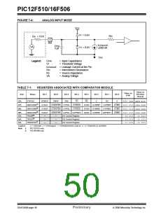
ANALOG MODE SELECTION
The ANS<1:0> bits are used to configure pins for
analog input. Upon any Reset, ANS<1:0> defaults to
11. This configures pins AN0, AN1 and AN2 as analog
inputs. The comparator output, C1OUT, will override
AN2 as an input if the comparator output is enabled.
Pins configured as analog inputs are not available for
digital output. Users should not change the ANS bits
while a conversion is in process. ANS bits are active
regardless of the condition of ADON.
The GO/DONE bit is cleared when the device enters
Sleep, stopping the current conversion. The ADC does
not have a dedicated oscillator, it runs off of the instruc-
tion clock. Therefore, no conversion can occur in sleep.
The GO/DONE bit cannot be set when ADON is clear.
9.1.3
ADC CHANNEL SELECTION
The CHS bits are used to select the analog channel to
be sampled by the ADC. The CHS<1:0> bits can be
changed at any time without adversely effecting a con-
version. To acquire an analog signal the CHS<1:0>
selection must match one of the pin(s) selected by the
ANS<1:0> bits. When the ADC is on (ADON = 1) and a
channel is selected that is also being used by the
comparator, then both the comparator and the ADC will
see the analog voltage on the pin.
© 2006 Microchip Technology Inc.
Preliminary
DS41268B-page 51

 ETC [ ETC ]