PIC12F510/16F506
7.1
Comparator Operation
Note:
Analog levels on any pin that is defined as
a digital input may cause the input buffer
to consume more current than is specified.
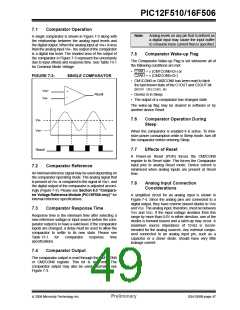
A single comparator is shown in Figure 7-3 along with
the relationship between the analog input levels and
the digital output. When the analog input at VIN+ is less
than the analog input VIN-, the output of the comparator
is a digital low level. The shaded area of the output of
the comparator in Figure 7-3 represent the uncertainty
due to input offsets and response time. See Table 13-1
for Common Mode Voltage.
7.5
Comparator Wake-up Flag
The Comparator Wake-up Flag is set whenever all of
the following conditions are met:
• C1WU = 0(CM1CON0<0>) or
C2WU = 0(CM2CON0<0>)
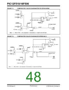
FIGURE 7-3:
SINGLE COMPARATOR
• CM1CON0 or CM2CON0 has been read to latch
the last known state of the C1OUT and C2OUT bit
(MOVF CM1CON0, W)
VIN+
VIN-
+
Result
• Device is in Sleep
–
• The output of a comparator has changed state
The wake-up flag may be cleared in software or by
another device Reset.
7.6
Comparator Operation During
Sleep
VIN-
VIN+
When the comparator is enabled it is active. To mini-
mize power consumption while in Sleep mode, turn off
the comparator before entering Sleep.
Result
7.7
Effects of Reset
A Power-on Reset (POR) forces the CM2CON0
register to its Reset state. This forces the Comparator
input pins to analog Reset mode. Device current is
minimized when analog inputs are present at Reset
time.
7.2
Comparator Reference
An internal reference signal may be used depending on
the comparator operating mode. The analog signal that
is present at VIN- is compared to the signal at VIN+, and
the digital output of the comparator is adjusted accord-
ingly (Figure 7-3). Please see Section 8.0 “Compara-
tor Voltage Reference Module (PIC16F506 only)” for
internal reference specifications.
7.8
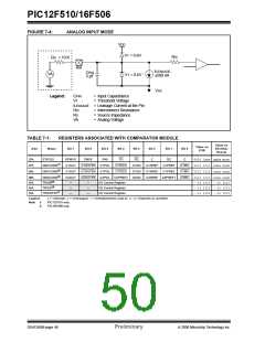
Analog Input Connection
Considerations
A simplified circuit for an analog input is shown in
Figure 7-4. Since the analog pins are connected to a
digital output, they have reverse biased diodes to VDD
and VSS. The analog input, therefore, must be between
VSS and VDD. If the input voltage deviates from this
range by more than 0.6V in either direction, one of the
diodes is forward biased and a latch-up may occur. A
maximum source impedance of 10 kΩ is recom-
mended for the analog sources. Any external compo-
nent connected to an analog input pin, such as a
capacitor or a Zener diode, should have very little
leakage current.
7.3
Comparator Response Time
Response time is the minimum time after selecting a
new reference voltage or input source before the com-
parator output is to have a valid level. If the comparator
inputs are changed, a delay must be used to allow the
comparator to settle to its new state. Please see
Table 13-1
specifications.
for
comparator
response
time
7.4
Comparator Output
The comparator output is read through the CM1CON0
or CM2CON0 register. This bit is read-only. The
comparator output may also be used externally, see
Figure 7-3.
© 2006 Microchip Technology Inc.
Preliminary
DS41268B-page 47

 ETC [ ETC ]