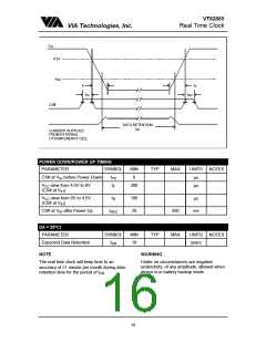
VT82885
Real Time Clock
VIA Technologies, Inc.
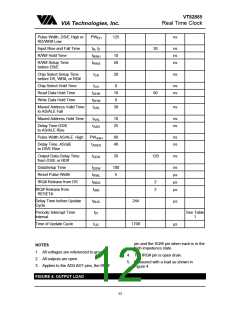
Pulse Width, DS/E High or
RD/WR# Low
PW
125
ns
EH
Input Rise and Fall Time
R/W# Hold Time
t , t
30
ns
ns
ns
R
F
t
10
50
RWH
R/W# Setup Time
before DS/E
t
RWS
Chip Select Setup Time
before DS, WR#, or RD#
t
20
ns
CS
Chip Select Hold Time
Read Data Hold Time
Write Data Hold Time
t
0
10
0
ns
ns
CH
t
80
DHR
t
DHW
Muxed Address Valid Time
to AS/ALE Fall
t
30
ns
ASL
Muxed Address Hold Time
t
10
25
ns
ns
AHL
Delay Time DS/E
to AS/ALE Rise
t
ASD
Pulse Width AS/ALE High
PW
ASH
t
ASED
60
40
ns
ns
Delay Time, AS/alE
to DS/E Rise
Output Data Delay Time
from DS/E or RD#
t
20
120
ns
DDR
DataSetup Time
t
100
5
ns
µs
µs
µs
DSW
Reset Pulse Width
IRQ# Release from DS
t
RWL
t
2
2
IRDS
IRQ# Release from
RESET#
t
IRR
Delay Time before Update
Cycle
t
244
µs
BUC
Periodic Interrupt Time
Interval
t
PI
See Table
1
Time of Update Cycle
t
1708
µs
UC
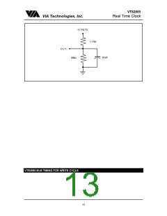
pin and the SQW pin when each is in the
high impedence state.
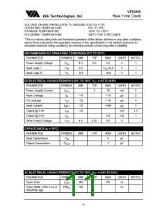
NOTES
1. All voltages are referenced to ground.
2. All outputs are open.
4. The IRQ# pin is open drain.
5. Measured with a load as shown in
Figure 4.
3. Applies to the AD0-AD7 pins, the IRQ#
FIGURE 4: OUTPUT LOAD
12

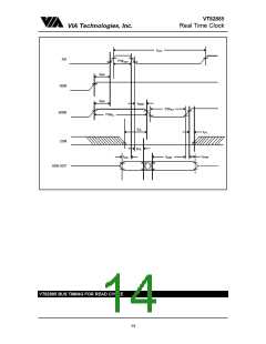
 ETC [ ETC ]
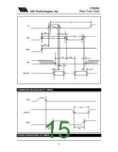