Data Sheet
June 2002
TMXF28155 Supermapper
155/51 Mbits/s SONET/SDH x28/x21 DS1/E1
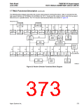
17 TMUX Functional Description (continued)
17.3.3 Receive MSP 1 + 1 Payload Switch
Output from both receive framer blocks provides the input to the MSP 1 + 1 payload switch. This portion of the
TMUX implements a payload 1 + 1 protection switch. In the receive direction, this occurs prior to pointer interpreta-
tion. If the protection switch is activated, then the data is selected from the receive protection interface rather than
from the high-speed input path. Only the selected input traffic is provided downstream to the pointer interpreter.
The interface consists of a 155.52 MHz or 51.84 MHz clock, data, and sync pulse.
17.3.4 Receive Pointer Interpreter
The pointer interpreter is implemented via a state machine which implements the pointer interpretation algorithm
described in ETS 300 417-1-1: January 1996-Annex B. The pointer interpreter evaluates the current pointer state
for the normal state, path AIS state, or LOP conditions, as well as pointer increments and decrements. The current
pointer state and any changes in pointer condition are reported to the control system. The number of consecutive
frames for invalid pointer and invalid concatenation indication is fixed at 9.
17.3.5 Receive High-Order Path Overhead Termination and RPOAC Drop
Path overhead (POH) termination is performed in the receive path on either all three STS-1s or on the VC-4 POH
only. The receive POH circuitry includes J1 byte monitoring, B3 byte BIP-8 checking, C2 byte signal label monitor-
ing, REI-P and RDI-P detection, H4 byte multiframe monitoring; F2, F3, and K3 byte APS monitoring, N1 byte tan-
dem connection monitoring (TCM), signal degrade BER and signal fail BER detection; receive path overhead
access channel (RPOAC) drop, and AIS-P/HO-AIS insertion and automatic AIS generation (with individual inhibit).
The J1 monitor provides five modes of operation for a programmable length (1 byte to 64 bytes) of the trace identi-
fier. These five modes are comprised of cyclic checking against the last received sequence, compare against a
programmed sequence, SONET framing mode, SDH framing mode, and consecutive consistent occurrences of a
new pattern. B3 is monitored either in bit or block mode. Provisionable N-times detection counters are imple-
mented for the C2, F2, F3, N1, and K3 bytes. The K3 APS byte and N1 TCM byte can be monitored as an entire
8-bit word or two 4-bit nibbles.
The receive RPOAC provides access to all the path overhead bytes. Even or odd parity is calculated over all bytes.
The RPOAC has a data rate of 9 bytes per 8 kHz frame and consists of clock, data, and an 8 kHz sync pulse.
17.3.6 Receive Byte Interleave Demultiplexer
The byte interleave demultiplexer accepts serial traffic and demultiplexes that information into one (STS-1 mode)
or three (STS-3/STM-1 mode) traffic streams for input via the telecom bus to the VT/VC mapper. The demultiplexer
takes the bytes in the order they are presented and places that traffic onto the telecom bus.
17.3.7 Receive Telecom Bus
The TMUX can communicate with up to three SPE mappers via the telecom bus interface. In typical applications,
since one SPE mapper is included in the Supermapper device, two external SPE mappers reside on the telecom
bus. The bus operates at 19.44 MHz for STS-3/STM-1 modes and at 6.48 MHz for STS-1 mode. In the receive
direction, the Supermapper outputs one parallel clock at 19.44 MHz, three sync signals (SPE, J0J1V1, and V1), an
8-bit data bus, and an odd/even parity bit. The data bus carries either three STS-1/TUG-3 signals, each in their
own time slot, or it carries one STS-1 signal. A 51.84 MHz low-speed clock and sync signal is also output from this
circuit.
Agere Systems Inc.
369

 ETC [ ETC ]