PRELIMINARY PRODUCT SPECIFICATION
nRF24L01 Single Chip 2.4 GHz Radio Transceiver
DEVICE CONFIGURATION
All configuration of nRF24L01 is defined by values in some configuration registers.
All these registers are writable via the SPI interface.
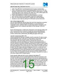
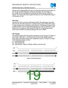
SPI Interface
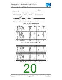
The SPI interface is a standard SPI interface with a maximum data rate of 10Mbps.
Most registers are readable.
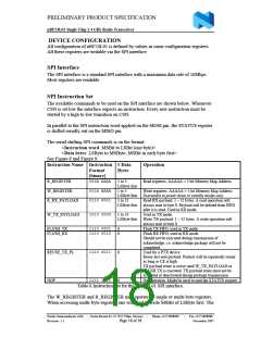
SPI Instruction Set
The available commands to be used on the SPI interface are shown below. Whenever
CSN is set low the interface expects an instruction. Every new instruction must be
started by a high to low transition on CSN.
In parallel to the SPI instruction word applied on the MOSI pin, the STATUS register
is shifted serially out on the MISO pin.
The serial shifting SPI commands is on the format:
<Instruction word: MSBit to LSBit (one byte)>
<Data bytes: LSByte to MSByte, MSBit in each byte first>
See Figure 8 and Figure 9.
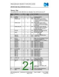
Instruction Name Instruction # Data
Operation
Format
Bytes
[binary]
000A AAAA
R_REGISTER
1 to 5
LSByte first
1 to 5
Read registers. AAAAA = 5 bit Memory Map Address
Write registers. AAAAA = 5 bit Memory Map Address
001A AAAA
0110 0001
W_REGISTER
R_RX_PAYLOAD
LSByte first Executable in power down or standby modes only.
1 to 32 Read RX-payload: 1 – 32 bytes. A read operation will
LSByte first always start at byte 0. Payload will be deleted from FIFO
after it is read. Used in RX mode.
1010 0000
W_TX_PAYLOAD
1 to 32
Used in TX mode.
LSByte first Write TX-payload: 1 – 32 bytes. A write operation will
always start at byte 0.
1110 0001
1110 0010
FLUSH_TX
FLUSH_RX
0
0
Flush TX FIFO, used in TX mode
Flush RX FIFO, used in RX mode
Should not be executed during transmission of
acknowledge, i.e. acknowledge package will not be
completed.
1110 0011
REUSE_TX_PL
0
Used for a PTX device
Reuse last sent payload. Packets will be repeatedly resent
as long as CE is high.
TX payload reuse is active until W_TX_PAYLOAD or
FLUSH TX is executed. TX payload reuse must not be
activated or deactivated during package transmission
No Operation. Might be used to read the STATUS register
1111 1111
NOP
0
Table 8 Instruction set for the nRF24L01 SPI interface.
The W_REGISTER and R_REGISTER may operate on single or multi-byte registers.
When accessing multi-byte registers one will read or write MSBit of LSByte first. The
Nordic Semiconductor ASA - Vestre Rosten 81, N-7075 Tiller, Norway
Revision: 1.1
-
Phone +4772898900
-
Fax +4772898989
November 2005
Page 18 of 38

 ETC [ ETC ]