PRELIMINARY PRODUCT SPECIFICATION
nRF24L01 Single Chip 2.4 GHz Radio Transceiver
writing can be terminated before all bytes in a multi-byte register has been written. In
this case the unwritten MSByte(s) will remain unchanged. E.g. the LSByte of
RX_ADDR_P0 can be modified by writing only one byte to the RX_ADDR_P0
register. The content of the status register will always be read to MISO after a high to
low transition on CSN.
Interrupt
The nRF24L01 has an active low interrupt pin (IRQ). The interrupt pin is activated
when TX_DS, RX_DR or MAX_RT is set high in status register. When MCU writes
'1' to the interrupt source, the IRQ pin will go inactive. The interrupt mask part of the
CONFIG register is used to mask out the interrupt sources that are allowed to set the
IRQ pin low. By setting one of the MASK bits high, the corresponding interrupt
source will be disabled. By default all interrupt sources are enabled.
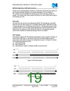
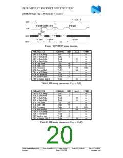
SPI Timing
The interface supports SPI. SPI operation and timing is given in Figure 8 to Figure 10
and in Table 9 and Table 10. The device must be in one of the standby modes or
power down mode before writing to the configuration registers. In Figure 8 to Figure
10 the following notations are used:
Cn – SPI Instruction Bit
Sn – Status Register Bit
Dn – Data Bit (note: LSByte to MSByte, MSBit in each byte first)
CSN
SCK
C7
S7
C6
S6
C5
S5
C4
S4
C3
S3
C2
S2
C1
S1
C0
S0
MOSI
MISO
D7
D6
D5
D4
D3
D2
D1
D0
D15
D14 D13 D12 D11 D10 D9
D8
Figure 8 SPI read operation.
CSN
SCK
MOSI
MISO
C7
C6
C5
C4
C3
S3
C2
S2
C1
S1
C0
S0
D7
D6
D5
D4
D3
D2
D1
D0
D15
D14 D13 D12 D11 D10 D9
D8
S7
S6
S5
S4
Figure 9 SPI write operation.
Nordic Semiconductor ASA - Vestre Rosten 81, N-7075 Tiller, Norway
Revision: 1.1
-
Phone +4772898900
-
Fax +4772898989
November 2005
Page 19 of 38

 ETC [ ETC ]