a-Si TFT LCD Single Chip Driver
240RGBx320 Resolution and 262K color
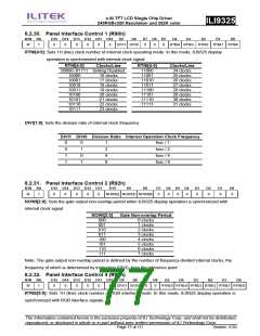
ILI9325
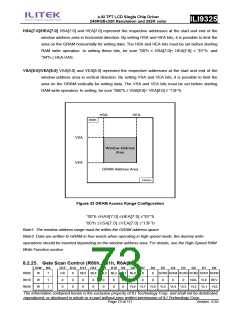
HSA[7:0]/HEA[7:0] HSA[7:0] and HEA[7:0] represent the respective addresses at the start and end of the
window address area in horizontal direction. By setting HSA and HEA bits, it is possible to limit the
area on the GRAM horizontally for writing data. The HSA and HEA bits must be set before starting
RAM write operation. In setting these bits, be sure “00”h ≤ HSA[7:0]< HEA[7:0] ≤ “EF”h. and
“04”h≦HEA-HAS.
VSA[8:0]/VEA[8:0] VSA[8:0] and VEA[8:0] represent the respective addresses at the start and end of the
window address area in vertical direction. By setting VSA and VEA bits, it is possible to limit the
area on the GRAM vertically for writing data. The VSA and VEA bits must be set before starting
RAM write operation. In setting, be sure “000”h ≤ VSA[8:0]< VEA[8:0] ≤ “13F”h.
HSA
HEA
0000h
VSA
VEA
Window Address
Area
GRAM Address Area
13FEFh
Figure 32 GRAM Access Range Configuration
“00”h ≤HAS[7:0] ≤HEA[7:0] ≤”EF”h
“00”h ≤VSA[7:0] ≤VEA[7:0] ≤”13F”h
Note1. The window address range must be within the GRAM address space.
Note2. Data are written to GRAM in four-words when operating in high speed mode, the dummy write
operations should be inserted depending on the window address area. For details, see the High-Speed RAM
Write Function section.
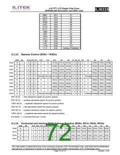
8.2.25. Gate Scan Control (R60h, R61h, R6Ah)
R/W RS
D15 D14 D13 D12 D11 D10 D9
D8
D7
D6
D5
D4
D3
D2
D1
D0
R60h
R61h
R6Ah
W
W
W
1
1
1
GS
0
0
0
0
NL5 NL4 NL3 NL2 NL1 NL0
0
0
SCN5 SCN4 SCN3 SCN2 SCN1 SCN0
0
0
0
0
0
0
0
0
0
0
0
0
0
0
0
0
NDL VLE REV
0
VL8 VL7 VL6 VL5 VL4 VL3 VL2 VL1 VL0
The information contained herein is the exclusive property of ILI Technology Corp. and shall not be distributed,
reproduced, or disclosed in whole or in part without prior written permission of ILI Technology Corp.
Page 73 of 111
Version: 0.35

 ETC [ ETC ]