a-Si TFT LCD Single Chip Driver
240RGBx320 Resolution and 262K color
ILI9325
0
0
0
1
1
1
1
0
1
1
0
0
1
1
1
0
1
0
1
0
1
Fosc / 2
Fosc / 4
0
0
0
1
1
1
1
0
1
1
0
0
1
1
1
0
1
0
1
0
1
Fosc / 8
Fosc / 16
Fosc / 32
Fosc / 8
Fosc / 16
Fosc / 64
Fosc / 32
Fosc / 128
Fosc / 64
Fosc / 256
Halt step-up circuit 1
Halt step-up circuit 2
Note: Be sure fDCDC1≥fDCDC2 when setting DC0[2:0] and DC1[2:0].
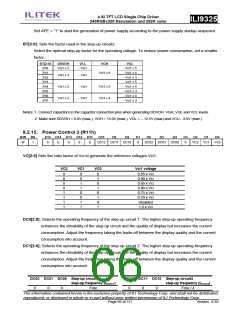
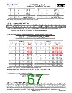
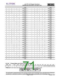
8.2.16. Power Control 3 (R12h)
R/W RS
D15 D14 D13 D12 D11 D10 D9 D8
D7
VCIRE
D6 D5
D4
D3
D2
D1
D0
W
1
0
0
0
0
0
0
0
0
0
0
PON VRH3 VRH2 VRH1 VRH0
VRH[3:0] Set the amplifying rate (1.6 ~ 1.9) of Vci applied to output the VREG1OUT level, which is a
reference level for the VCOM level and the grayscale voltage level.
VCIRE: Select the external reference voltage Vci or internal reference voltage VCIR.
VCIRE=0
VCIRE =1
External reference voltage Vci (default)
Internal reference voltage 2.5V
VCIRE =0
VCIRE =1
VRH3 VRH2 VRH1 VRH0
VRH3 VRH2 VRH1 VRH0 VREG1OUT
VREG1OUT
0
0
0
0
0
0
0
0
1
1
1
1
1
1
1
1
0
0
0
0
1
1
1
1
0
0
0
0
1
1
1
1
0
0
1
1
0
0
1
1
0
0
1
1
0
0
1
1
0
1
0
1
0
1
0
1
0
1
0
1
0
1
0
1
Halt
0
0
0
0
0
0
0
0
1
1
1
1
1
1
1
1
0
0
0
0
1
1
1
1
0
0
0
0
1
1
1
1
0
0
1
1
0
0
1
1
0
0
1
1
0
0
1
1
0
1
0
1
0
1
0
1
0
1
0
1
0
1
0
1
Halt
Vci x 2.00
Vci x 2.05
Vci x 2.10
Vci x 2.20
Vci x 2.30
Vci x 2.40
Vci x 2.40
Vci x 1.60
Vci x 1.65
Vci x 1.70
Vci x 1.75
Vci x 1.80
Vci x 1.85
Vci x 1.90
Vci x 1.95
2.5V x 2.00 = 5.000V
2.5V x 2.05 = 5.125V
2.5V x 2.10 = 5.250V
2.5V x 2.20 = 5.500V
2.5V x 2.30 = 5.750V
2.5V x 2.40 = 6.000V
2.5V x 2.40 = 6.000V
2.5V x 1.60 = 4.000V
2.5V x 1.65 = 4.125V
2.5V x 1.70 = 4.250V
2.5V x 1.75 = 4.375V
2.5V x 1.80 = 4.500V
2.5V x 1.85 = 4.625V
2.5V x 1.90 = 4.750V
2.5V x 1.95 = 4.875V
When VCI<2.5V, Internal reference voltage will be same as VCI.
Make sure that VC and VRH setting restriction: VREG1OUT ≦ (DDVDH - 0.5)V.
PON: Control ON/OFF of circuit3 (VGL) output.
PON=0
PON=1
VGL output is disable
VGL output is enable
8.2.17. Power Control 4 (R13h)
R/W
RS
D15
D14
D13
D12
D11
D10
D9
D8
D7
D6
D5
D4
D3
D2 D1 D0
W
1
0
0
0
VDV4 VDV3 VDV2 VDV1 VDV0
0
0
0
0
0
0
0
0
The information contained herein is the exclusive property of ILI Technology Corp. and shall not be distributed,
reproduced, or disclosed in whole or in part without prior written permission of ILI Technology Corp.
Page 67 of 111
Version: 0.35

 ETC [ ETC ]