a-Si TFT LCD Single Chip Driver
240RGBx320 Resolution and 262K color
ILI9325
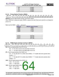
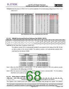
VDV[4:0] Select the factor of VREG1OUT to set the amplitude of Vcom alternating voltage from 0.70 to 1.24 x
VREG1OUT .
VDV4 VDV3VDV2 VDV1 VDV0
VCOM amplitude
VREG1OUT x 0.70
VREG1OUT x 0.72
VREG1OUT x 0.74
VREG1OUT x 0.76
VREG1OUT x 0.78
VREG1OUT x 0.80
VREG1OUT x 0.82
VREG1OUT x 0.84
VREG1OUT x 0.86
VREG1OUT x 0.88
VREG1OUT x 0.90
VREG1OUT x 0.92
VREG1OUT x 0.94
VREG1OUT x 0.96
VREG1OUT x 0.98
VREG1OUT x 1.00
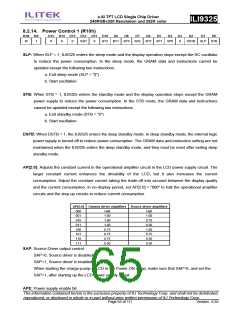
VDV4 VDV3VDV2 VDV1 VDV0
VCOM amplitude
VREG1OUT x 0.94
VREG1OUT x 0.96
VREG1OUT x 0.98
VREG1OUT x 1.00
VREG1OUT x 1.02
VREG1OUT x 1.04
VREG1OUT x 1.06
VREG1OUT x 1.08
VREG1OUT x 1.10
VREG1OUT x 1.12
VREG1OUT x 1.14
VREG1OUT x 1.16
VREG1OUT x 1.18
VREG1OUT x 1.20
VREG1OUT x 1.22
VREG1OUT x 1.24
0
0
0
0
0
0
0
0
0
0
0
0
0
0
0
0
0
0
0
0
0
0
0
0
1
1
1
1
1
1
1
1
0
0
0
0
1
1
1
1
0
0
0
0
1
1
1
1
0
0
1
1
0
0
1
1
0
0
1
1
0
0
1
1
0
1
0
1
0
1
0
1
0
1
0
1
0
1
0
1
1
1
1
1
1
1
1
1
1
1
1
1
1
1
1
1
0
0
0
0
0
0
0
0
1
1
1
1
1
1
1
1
0
0
0
0
1
1
1
1
0
0
0
0
1
1
1
1
0
0
1
1
0
0
1
1
0
0
1
1
0
0
1
1
0
1
0
1
0
1
0
1
0
1
0
1
0
1
0
1
Set VDV[4:0] to let Vcom amplitude less than 6V.
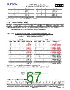
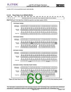
8.2.18. GRAM Horizontal/Vertical Address Set (R20h, R21h)
R/W RS
D15 D14 D13 D12 D11 D10 D9
D8
D7
D6
D5
D4
D3
D2
D1
D0
W
W
1
1
0
0
0
0
0
0
0
0
0
0
0
0
0
0
0
AD7
AD6
AD5
AD4
AD3
AD2
AD1 AD0
AD16 AD15 AD14 AD13 AD12 AD11 AD10 AD9 AD8
AD[16:0] Set the initial value of address counter (AC).
The address counter (AC) is automatically updated in accordance to the setting of the AM, I/D bits
as data is written to the internal GRAM. The address counter is not automatically updated when
read data from the internal GRAM.
AD[16:0]
GRAM Data Map
1st line GRAM Data
2nd line GRAM Data
3rd line GRAM Data
4th line GRAM Data
17’h00000 ~ 17’h000EF
17’h00100 ~ 17’h001EF
17’h00200 ~ 17’h002EF
17’h00300 ~ 17’h003EF
17’h13D00 ~ 17’ h13DEF
17’h13E00 ~ 17’ h13EEF
17’h13F00 ~ 17’h13FEF
318th line GRAM Data
319th line GRAM Data
320th line GRAM Data
Note1: When the RGB interface is selected (RM = “1”), the address AD[16:0] is set to the address counter
every frame on the falling edge of VSYNC.
Note2: When the internal clock operation or the VSYNC interface mode is selected (RM = “0”), the address
AD[16:0] is set to address counter when update register R21.
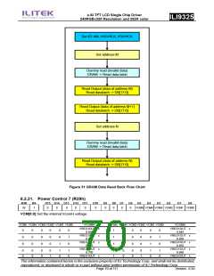
8.2.19. Write Data to GRAM (R22h)
R/W RS
D17 D16 D15 D14 D13 D12 D11 D10 D9 D8 D7 D6 D5 D4 D3 D2 D1 D0
W
1
RAM write data (WD[17:0], the DB[17:0] pin assignment differs for each interface.
This register is the GRAM access port. When update the display data through this register, the address
The information contained herein is the exclusive property of ILI Technology Corp. and shall not be distributed,
reproduced, or disclosed in whole or in part without prior written permission of ILI Technology Corp.
Page 68 of 111
Version: 0.35

 ETC [ ETC ]