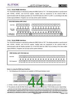
a-Si TFT LCD Single Chip Driver
240RGBx320 Resolution and 262K color
ILI9325
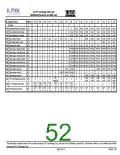
8. Register Descriptions
8.1. Registers Access
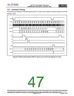
ILI9325 adopts 18-bit bus interface architecture for high-performance microprocessor. All the functional
blocks of ILI9325 starts to work after receiving the correct instruction from the external microprocessor by the
18-, 16-, 9-, 8-bit interface. The index register (IR) stores the register address to which the instructions and
display data will be written. The register selection signal (RS), the read/write signals (nRD/nWR) and data
bus D17-0 are used to read/write the instructions and data of ILI9325. The registers of the ILI9325 are
categorized into the following groups.
1. Specify the index of register (IR)
2. Read a status
3. Display control
4. Power management Control
5. Graphics data processing
6. Set internal GRAM address (AC)
7. Transfer data to/from the internal GRAM (R22)
8. Internal grayscale γ-correction (R30 ~ R39)
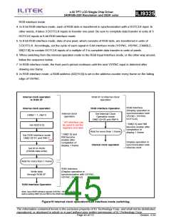
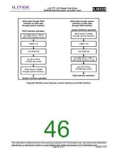
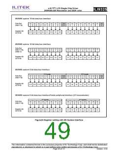
Normally, the display data (GRAM) is most often updated, and in order since the ILI9325 can update internal
GRAM address automatically as it writes data to the internal GRAM and minimize data transfer by using the
window address function, there are fewer loads on the program in the microprocessor. As the following figure
shows, the way of assigning data to the 16 register bits (D[15:0]) varies for each interface. Send registers in
accordance with the following data transfer format.
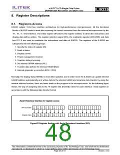
Serial Peripheral Interface for register access
D
D
D
D
D
D
D
9
D
8
D
7
D
6
D
5
D
4
D
3
D
2
D
1
D
0
SPI Input Data
Register Data
15
14
13
12
11
10
D
15
D
14
D
13
D
12
D
11
D
10
D
9
D
8
D
7
D
6
D
5
D
4
D
3
D
2
D
1
D
0
Figure22 Register Setting with Serial Peripheral Interface (SPI)
The information contained herein is the exclusive property of ILI Technology Corp. and shall not be distributed,
reproduced, or disclosed in whole or in part without prior written permission of ILI Technology Corp.
Page 48 of 111
Version: 0.35

 ETC [ ETC ]