a-Si TFT LCD Single Chip Driver
240RGBx320 Resolution and 262K color
ILI9325
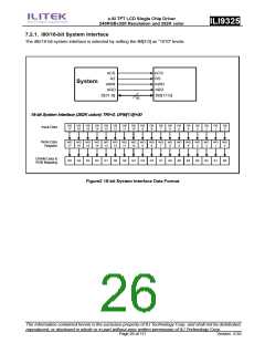
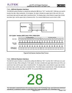
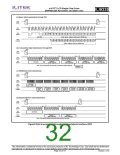
7.2.3. i80/9-bit System Interface
The i80/9-bit system interface is selected by setting the IM[3:0] as “1011” and the DB17~DB9 pins are used to
transfer the data. When writing the 16-bit register, the data is divided into upper byte (8 bits and LSB is not
used) lower byte and the upper byte is transferred first. The display data is also divided in upper byte (9 bits)
and lower byte, and the upper byte is transferred first. The unused DB[8:0] pins must be tied to GND.
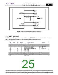
nCS
A1
nCS
RS
System
nWR
nRD
D[8:0]
nWR
nRD
DB[17:9]
9
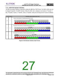
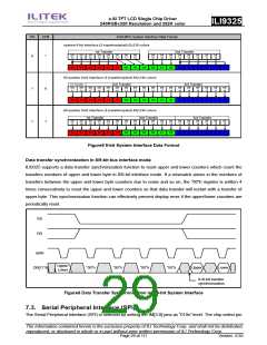
9-bit System Interface (262K colors) TRI=0, DFM[1:0]=00
1st Transfer (Upper bits)
2nd Transfer (Lower bits)
DB
17
DB
16
DB
15
DB
14
DB
13
DB
12
DB
11
DB
10
DB
9
DB
17
DB
16
DB
15
DB
14
DB
13
DB
12
DB
11
DB
10
DB
9
Input Data
Write Data
Register
WD WD WD WD WD WD WD WD WD WD WD WD WD WD WD WD WD WD
17
16
15
14
13
12
11
10
9
8
7
6
5
4
3
2
1
0
GRAM Data &
RGB Mapping
R5
R4
R3
R2
R1
R0
G5
G4
G3
G2
G1
G0
B5
B4
B3
B2
B1
B0
Figure4 9-bit System Interface Data Format
7.2.4. i80/8-bit System Interface
The i80/8-bit system interface is selected by setting the IM[3:0] as “0011” and the DB17~DB10 pins are used
to transfer the data. When writing the 16-bit register, the data is divided into upper byte (8 bits and LSB is not
used) lower byte and the upper byte is transferred first. The display data is also divided in upper byte (8 bits)
and lower byte, and the upper byte is transferred first. The written data is expanded into 18 bits internally (see
the figure below) and then written into GRAM. The unused DB[9:0] pins must be tied to GND.
The information contained herein is the exclusive property of ILI Technology Corp. and shall not be distributed,
reproduced, or disclosed in whole or in part without prior written permission of ILI Technology Corp.
Page 28 of 111
Version: 0.35

 ETC [ ETC ]