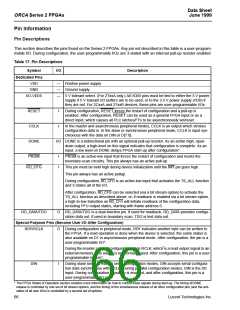
Data Sheet
June 1999
ORCA Series 2 FPGAs
Pin Information (continued)
Table 17. Pin Descriptions (continued)
Symbol
I/O
Description
Special-Purpose Pins Special-Purpose Pins (Become User I/O After Configuration) (continued)
M0, M1, M2
M3
I
I
During powerup and initialization, M0—M2 are used to select the configuration mode
with their values latched on the rising edge of INIT. See Table 7 for the configuration
modes. During configuration, a pull-up is enabled, and after configuration, the pins are
user-programmable I/O*.
During powerup and initialization, M3 is used to select the speed of the internal oscilla-
tor during configuration, with its value latched on the rising edge of INIT. When M3 is
low, the oscillator frequency is 10 MHz. When M3 is high, the oscillator is 1.25 MHz.
During configuration, a pull-up is enabled, and after configuration, this pin is a user-pro-
grammable I/O pin*.
TDI, TCK, TMS
I
If boundary scan is used, these pins are Test Data In, Test Clock, and Test Mode Select
inputs. If boundary scan is not selected, all boundary-scan functions are inhibited once
configuration is complete, and these pins are user-programmable I/O pins. Even if
boundary scan is not used, either TCK or TMS must be held at logic 1 during configura-
tion. Each pin has a pull-up enabled during configuration*.
HDC
LDC
INIT
O
O
High During Configuration is output high until configuration is complete. It is used as a
control output indicating that configuration is not complete. After configuration, this pin is
a user-programmable I/O pin*.
Low During Configuration is output low until configuration is complete. It is used as a
control output indicating that configuration is not complete. After configuration, this pin is
a user-programmable I/O pin*.
I/O INIT is a bidirectional signal before and during configuration. During configuration, a
pull-up is enabled, but an external pull-up resistor is recommended. As an active-low
open-drain output, INIT is held low during power stabilization and internal clearing of
memory. As an active-low input, INIT holds the FPGA in the wait-state before the start of
configuration. After configuration, the pin is a user-programmable I/O pin*.
CS0, CS1, WR, RD
I
CS0, CS1, WR, RD are used in the asynchronous peripheral configuration modes. The
FPGA is selected when CS0 is low and CS1 is high. When selected, a low on the write
strobe, WR, loads the data on D[7:0] inputs into an internal data buffer. WR, CS0, and
CS1 are also used as chip selects in the slave parallel mode.
A low on RD changes D7 into a status output. As a status indication, a high indicates
ready and a low indicates busy. WR and RD should not be used simultaneously. If they
are, the write strobe overrides. During configuration, a pull-up is enabled, and after con-
figuration, the pins are user-programmable I/O pins*.
A[17:0]
D[7:0]
DOUT
O
I
During master parallel configuration mode, A[17:0] address the configuration EPROM.
During configuration, a pull-up is enabled, and after configuration, the pins are user-
programmable I/O pins*.
During master parallel, peripheral, and slave parallel configuration modes, D[7:0]
receive configuration data and each pin has a pull-up enabled. After configuration, the
pins are user-programmable I/O pins*.
O
During configuration, DOUT is the serial data output that can drive the DIN of daisy-
chained slave LCA devices. Data out on DOUT changes on the falling edge of CCLK.
After configuration, DOUT is a user-programmable I/O pin*.
* The FPGA States of Operation section contains more information on how to control these signals during start-up. The timing of DONE
release is controlled by one set of bit stream options, and the timing of the simultaneous release of all other configuration pins (and the acti-
vation of all user I/Os) is controlled by a second set of options.
Lucent Technologies Inc.
67

 ETC [ ETC ]