Data Sheet
June 1999
ORCA Series 2 FPGAs
for each available package, and Table 18B provides the
number of user I/Os available in the ORCA OR2TxxA
series. It should be noted that the number of user I/Os
available for the OR2TxxA series is reduced from the
equivalent OR2CxxA devices by the number of
required VDD5 pins, as shown in Table 18B. The pins
that are converted from user I/O to VDD5 are denoted
as I/O-VDD5 in the pin information tables (Table 19
through 28). Each package has six dedicated configu-
ration pins.
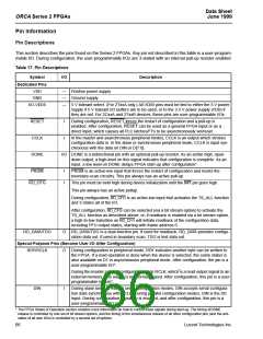
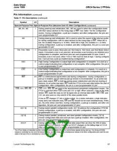
Pin Information (continued)
Package Compatibility
The package pinouts are consistent across ORCA
Series FPGAs with the following exception: some user
I/O pins that do not have any special functions will
be converted to VDD5 pins for the OR2TxxA series.
If the designer does not use these pins for the
OR2CxxA and OR2TxxB series, then pinout compati-
bility will be maintained between the ORCA OR2CxxA,
OR2TxxA, and OR2TxxB series of FPGAs. Note that
they must be connected to a power supply for the
OR2TxxA series.
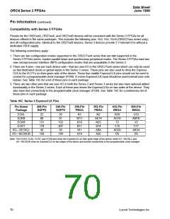
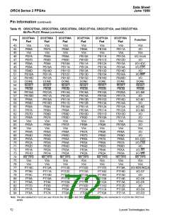
Table 19—Table 28. provide the package pin and pin
function for the ORCA Series 2 FPGAs and packages.
The bond pad name is identified in the PIC nomencla-
ture used in the ORCA Foundry design editor.
Package pinouts being consistent across all ORCA
Series FPGAs enables a designer to select a package
based on I/O requirements and change the FPGA with-
out laying out the printed-circuit board again. The
change might be to a larger FPGA if additional func-
tionality is needed, or it might be to a smaller FPGA to
decrease unit cost.
When the number of FPGA bond pads exceeds the
number of package pins, bond pads are unused. When
the number of package pins exceeds the number of
bond pads, package pins are left unconnected (no
connects). When a package pin is to be left as a no
connect for a specific die, it is indicated as a note in the
device pad column for the FPGA. The tables provide no
information on unused pads.
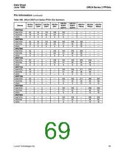
Table 18A provides the number of user I/Os available
for the ORCA OR2CxxA and OR2TxxB Series FPGAs
Table 18A. ORCA OR2CxxA and OR2TxxB Series FPGA I/Os Summary
208-Pin 240-Pin
304-Pin
SQFP/
SQFP2
84-Pin 100-Pin 144-Pin 160-Pin
256-Pin
PBGA
352-Pin 432-Pin
Device
SQFP/
SQFP2
SQFP/
SQFP2
PLCC
TQFP
TQFP
QFP
PBGA
EBGA
OR2C04A
User I/Os
VDD/VSS
OR2C06A
User I/Os
VDD/VSS
OR2C08A
User I/Os
VDD/VSS
OR2C10A
User I/Os
VDD/VSS
OR2C12A
User I/Os
VDD/VSS
64
14
77
17
114
24
130
24
160
31
—
—
—
—
—
—
—
—
—
—
64
14
77
17
114
24
130
24
171
31
192
42
192
26
—
—
—
—
—
—
64
14
—
—
—
—
130
24
171
31
192
40
221
26
—
—
—
—
—
—
64
14
—
—
—
—
130
24
171
31
192
40
221
26
—
—
256
48
—
—
64
14
—
—
—
—
—
—
171
31
192
42
223
26
252
46
288
48
—
—
OR2C15A/OR2T15B
User I/Os
VDD/VSS
OR2C26A
User I/Os
VDD/VSS
64
14
—
—
—
—
—
—
171
31
192
42
223
26
252
46
298
48
320*
84
—
—
—
—
—
—
—
—
171
31
192
42
—
—
252
46
298
48
342
84
OR2C40A/OR2T40B
User I/Os
VDD/VSS
—
—
—
—
—
—
—
—
171
31
192
42
—
—
252
46
—
—
342
84
* 432 EBGA not available for OR2T15B
68
Lucent Technologies Inc.

 ETC [ ETC ]