Data Sheet
June 1999
ORCA Series 2 FPGAs
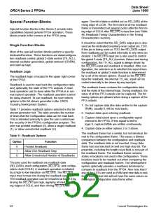
Special Function Blocks (continued)
s
TMS TDI
TCK
TDO
TMS TDI
TCK
TDO
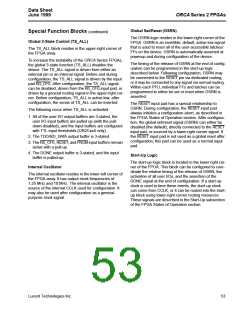
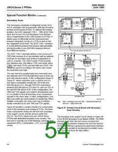
Boundary Scan
net a
net b
U2
U1
The increasing complexity of integrated circuits (ICs)
and IC packages has increased the difficulty of testing
printed-circuit boards (PCBs). To address this testing
problem, the IEEE standard 1149.1 - 1990 (IEEE Stan-
dard Test Access Port and Boundary-Scan Architec-
ture) is implemented in the ORCA series of FPGAs. It
allows users to efficiently test the interconnection
between integrated circuits on a PCB as well as test
the integrated circuit itself. The IEEE 1149.1 standard
is a well-defined protocol that ensures interoperability
among boundary-scan (BSCAN) equipped devices
from different vendors.
net c
TDI
TMS
TCK
TDO
TMS TDI
TCK
TDO
TMS TDI
TCK
TDO
U3
U4
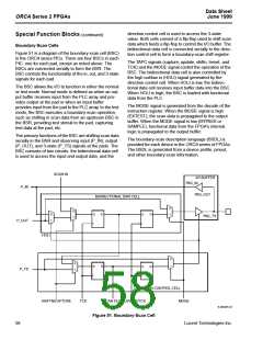
SEE ENLARGED VIEW BELOW
TDO TCK TMS TDI
The IEEE 1149.1 standard defines a test access port
(TAP) that consists of a 4-pin interface with an optional
reset pin for boundary-scan testing of integrated cir-
cuits in a system. The ORCA series FPGA provides
four interface pins: test data in (TDI), test mode select
(TMS), test clock (TCK), and test data out (TDO). The
PRGM pin used to reconfigure the device also resets
the boundary-scan logic.
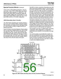
PT[ij]
TAPC
BSC
BDC DCC
SCAN
OUT
SCAN
IN
BYPASS
REGISTER
P_IN
P_TS
INSTRUCTION
REGISTER
P_OUT
SCAN
OUT
SCAN
IN
PR[ij]
BSC
P_IN
P_OUT
P_TS
The user test host serially loads test commands and
test data into the FPGA through these pins to drive out-
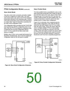
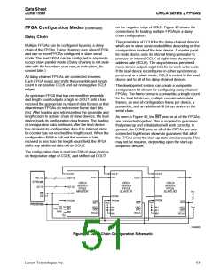
puts and examine inputs. In the configuration shown in
Figure 47, where boundary scan is used to test ICs,
test data is transmitted serially into TDI of the first
BSCAN device (U1), through TDO/TDI connections
between BSCAN devices (U2 and U3), and out TDO of
the last BSCAN device (U4). In this configuration, the
TMS and TCK signals are routed to all boundary-scan
ICs in parallel so that all boundary-scan components
operate in the same state. In other configurations, mul-
tiple scan paths are used instead of a single ring. When
multiple scan paths are used, each ring is indepen-
dently controlled by its own TMS and TCK signals.
P_TS
BSC
PLC
ARRAY
DCC
BDC
DCC
P_OUT
BDC
P_IN
PL[ij]
SCAN
IN
SCAN
OUT
P_OUT
P_TS
P_IN
BSC
DCC BDC
SCAN
OUT
SCAN
IN
PB[ij]
ENLARGED VIEW
Fig.34.a(F).1C
Key: BSC = boundary-scan cell, BDC = bidirectional data cell,
and DCC = data control cell.
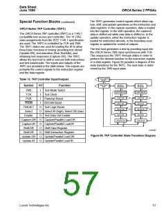
Figure 48 provides a system interface for components
used in the boundary-scan testing of PCBs. The three
major components shown are the test host, boundary-
scan support circuit, and the devices under test
(DUTs). The DUTs shown here are ORCA Series
FPGAs with dedicated boundary-scan circuitry. The
test host is normally one of the following: automatic test
equipment (ATE), a workstation, a PC, or a micropro-
cessor.
Figure 47. Printed-Circuit Board with Boundary-
Scan Circuitry
The boundary-scan support circuit shown in Figure 48
is the 497AA Boundary-Scan Master (BSM). The BSM
off-loads tasks from the test host to increase test
throughput. To interface between the test host and the
DUTs, the BSM has a general microprocessor interface
and provides parallel-to-serial/serial-to-parallel conver-
sion, as well as three 8K data buffers.
54
Lucent Technologies Inc.

 ETC [ ETC ]