Data Sheet
June 1999
ORCA Series 2 FPGAs
Timing Characteristics (continued)
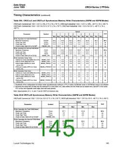
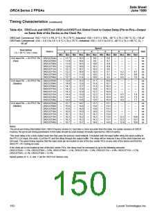
Table 39.B OR2TxxB Synchronous Memory Write Characteristics (SSPM and SDPM Modes) (continued)
OR2TxxB Commercial: VDD = 3.0 V to 3.6 V, 0 °C ≤ TA ≤ 70 °C; OR2TxxB Industrial: VDD = 3.0 V to 3.6 V, –40 °C ≤ TA ≤ +85°C.
Speed
Unit
Parameter
Symbol
-7
-8
Min
Max
Min
Max
Write Operation Setup Time:
Address to Clock (A[3:0]/B[3:0] to CK)
Data to Clock (WD[3:0] to CK)
Write Enable (WREN) to Clock
(A4 to CK)
MEMS_ASET
MEMS_DSET
MEMS_WRSET
0.0
0.0
0.0
—
—
—
0.0
0.0
0.0
—
—
—
ns
ns
ns
Write-port Enable (WPE) to Clock
(C0 to CK)
MEMS_PWRSET
0.0
—
0.0
—
ns
Write Operation Hold Time:
Address to Clock (A[3:0]/B[3:0] to CK)
Data to Clock (WD[3:0] to CK)
Write Enable (WREN) to Clock
(A4 to CK)
MEMS_AHLD
MEMS_DHLD
MEMS_WRHLD
1.0
1.0
1.0
—
—
—
0.8
0.8
0.8
—
—
—
ns
ns
ns
Write-port Enable (WPE) to Clock
(C0 to CK)
MEMS_PWRHLD
0.7
—
0.6
—
ns
1. Readback of the configuration bit stream when simultaneously writing to a PFU in either SSPM fast mode or SDPM fast mode is not allowed.
2. Because the setup time of data into the latches/FFs is less than 0 ns, data written into the RAM can be loaded into a latch/FF in the same
PFU on the next opposite clock edge (one-half clock period).
Note: Speed grades of -5, -6, and -7 are for OR2TxxA devices only.
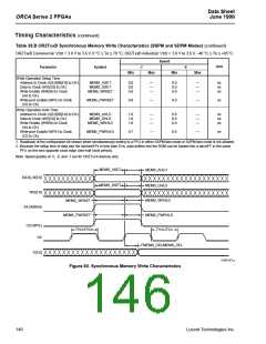
MEMS_ASET
MEMS_DSET
MEMS_AHLD
A[3:0], B[3:0]
WD[3:0]
MEMS_DHLD
MEMS_WRHLD
MEMS_PWRHLD
TFSCL/TSCL
MEMS_WRSET
MEMS_PWRSET
TFSCH/TSCH
A4 (WREN)
C0 (WPE)
CK
FMEMS_DEL/MEMS_DEL
F[3:0]
5-4621(F).a
Figure 60. Synchronous Memory Write Characteristics
146
Lucent Technologies Inc.

 ETC [ ETC ]