Data Sheet
June 1999
ORCA Series 2 FPGAs
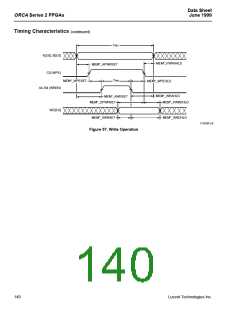
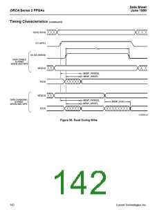
Timing Characteristics (continued)
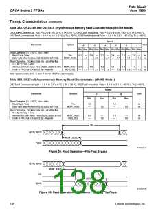
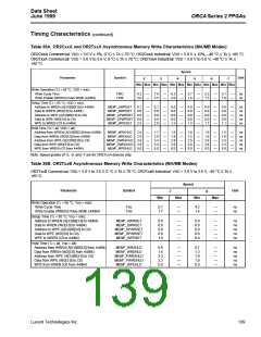
Table 36A. OR2CxxA and OR2TxxA Asynchronous Memory Write Characteristics (MA/MB Modes)
OR2CxxA Commercial: VDD = 5.0 V ± 5%, 0 °C ≤ TA ≤ 70 °C; OR2CxxA Industrial: VDD = 5.0 V ± 10%, –40 °C ≤ TA ≤ +85 °C.
OR2TxxA Commercial: VDD = 3.0 V to 3.6 V, 0 °C ≤ TA ≤ 70 °C; OR2TxxA Industrial: VDD = 3.0 V to 3.6 V, –40 °C ≤ TA ≤
+85 °C.
Speed
Parameter
Symbol
Unit
-2
-3
-4
-5
-6
-7
Min Max Min Max Min Max Min Max Min Max Min Max
Write Operation (TJ = 85 °C, VDD = min):
Write Cycle Time
Write Enable (WREN) Pulse Width (A4/B4)
TWC
TPW
9.3
3.0
—
—
7.8
2.5
—
—
6.3
2.0
—
—
5.7
1.8
—
—
5.2
1.7
—
—
5.1
1.6
—
—
ns
ns
Setup Time (TJ = 85 °C, VDD = min):
Address to WREN (A[3:0]/B[3:0] to A4/B4)
Data to WREN (WD[3:0] to A4/B4)
Address to WPE (A[3:0]/B[3:0] to C0)
Data to WPE (WD[3:0] to C0)
MEM*_AWRSET
MEM*_DWRSET
MEM*_APWRSET 0.0
MEM*_DPWRSET 0.0
0.1
0.0
—
—
—
—
—
0.1
0.0
0.0
0.0
2.0
—
—
—
—
—
0.0
0.0
0.0
0.0
1.5
—
—
—
—
—
0.0
0.0
0.0
0.0
1.4
—
—
—
—
—
0.0
0.0
0.0
0.0
1.1
—
—
—
—
—
0.0
0.0
0.0
0.0
1.1
—
—
—
—
—
ns
ns
ns
ns
ns
WPE to WREN (C0 to A4/B4)
MEM*_WPESET
2.5
Hold Time (TJ = all, VDD = all):
Address from WREN (A[3:0]/B[3:0] from A4/B4)
Data from WREN (WD[3:0] from A4/B4)
Address from WPE (A[3:0/B[3:0] to C0)
Data from WPE (WD[3:0] to C0)
MEM*_WRAHLD
MEM*_WRDHLD
MEM*_PWRAHLD 3.8
MEM*_PWRDHLD 3.9
2.4
2.4
—
—
—
—
—
1.7
2.0
3.3
3.4
0.0
—
—
—
—
—
1.8
1.9
2.8
2.9
0.0
—
—
—
—
—
1.6
1.5
2.5
2.6
0.0
—
—
—
—
—
1.6
1.6
2.4
2.4
0.0
—
—
—
—
—
1.5
1.6
2.3
2.3
0.0
—
—
—
—
—
ns
ns
ns
ns
ns
WPE from WREN (C0 from A4/B4)
MEM*_WPEHLD
0.0
Note: Speed grades of -5, -6, and -7 are for OR2TxxA devices only.
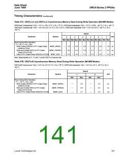
Table 36B. OR2TxxB Asynchronous Memory Write Characteristics (MA/MB Modes)
OR2TxxB Commercial: VDD = 3.0 V to 3.6 V, 0 °C ≤ TA ≤ 70 °C; OR2TxxB Industrial: VDD = 3.0 V to 3.6 V, –40 °C ≤ TA ≤
+85°C.
Speed
Parameter
Symbol
Unit
-7
-8
Min
Max
Min
Max
Write Operation (TJ = 85 °C, VDD = min):
Write Cycle Time
Write Enable (WREN) Pulse Width (A4/B4)
TWC
TPW
5.1
1.7
—
—
4.2
1.4
—
—
ns
ns
Setup Time (TJ = 85 °C, VDD = min):
Address to WREN (A[3:0]/B[3:0] to A4/B4)
Data to WREN (WD[3:0] to A4/B4)
Address to WPE (A[3:0]/B[3:0] to C0)
Data to WPE (WD[3:0] to C0)
MEM*_AWRSET
MEM*_DWRSET
MEM*_APWRSET
MEM*_DPWRSET
MEM*_WPESET
0.0
0.0
0.0
0.0
1.0
—
—
—
—
—
0.0
0.0
0.0
0.0
0.8
—
—
—
—
—
ns
ns
ns
ns
ns
WPE to WREN (C0 to A4/B4)
Hold Time (TJ = all, VDD = all):
Address from WREN (A[3:0]/B[3:0] from A4/B4)
Data from WREN (WD[3:0] from A4/B4)
Address from WPE (A[3:0/B[3:0] to C0)
Data from WPE (WD[3:0] to C0)
MEM*_WRAHLD
MEM*_WRDHLD
MEM*_PWRAHLD
MEM*_PWRDHLD
MEM*_WPEHLD
0.9
1.6
2.3
2.3
0.0
—
—
—
—
—
0.7
1.3
1.9
1.9
0.0
—
—
—
—
—
ns
ns
ns
ns
ns
WPE from WREN (C0 from A4/B4)
Lucent Technologies Inc.
139

 ETC [ ETC ]