Data Sheet
June 1999
ORCA Series 2 FPGAs
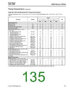
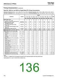
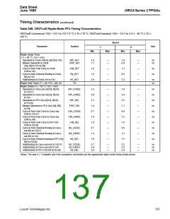
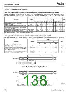
Timing Characteristics (continued)
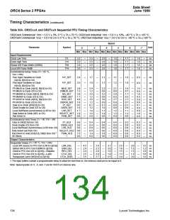
Table 33B. OR2TxxB Sequential PFU Timing Characteristics
OR2TxxB Commercial: VDD = 3.0 V to 3.6 V, 0 °C ≤ TA ≤ 70 °C; OR2TxxB Industrial: VDD = 3.0 V to 3.6 V, –40 °C ≤ TA ≤
+85°C.
Speed
Parameter
Symbol
Unit
-7
-8
Min
Max
Min
Max
Input Requirements
Clock Low Time
TCL
TCH
TRW
TPW
1.7
1.7
1.7
1.7
—
—
—
—
1.4
1.4
1.4
1.4
—
—
—
—
ns
ns
ns
ns
Clock High Time
Global S/R Pulse Width (GSRN)
Local S/R Pulse Width
Combinatorial Setup Times (TJ = 85 °C,
VDD = min):
Four Input Variables to Clock
(A[4:0], B[4:0] to CK)
Five Input Variables to Clock
(A[4:0], B[4:0] to CK)
F4*_SET
F5*_SET
1.0
1.0
—
—
0.8
0.8
—
—
ns
ns
PFUMUX to Clock (A[4:0], B[4:0] to CK)
PFUMUX to Clock (C0 to CK)
PFUNAND to Clock (A[4:0], B[4:0] to CK)
PFUNAND to Clock (C0 to CK)
PFUXOR to Clock (A[4:0], B[4:0] to CK)
PFUXOR to Clock (C0 to CK)
Data In to Clock (WD[3:0] to CK)
Clock Enable to Clock (CE to CK)
Local Set/Reset (synchronous) (LSR to CK)
Data Select to Clock (SEL to CK)
Pad Direct In
MUX_SET
C0MUX_SET
ND_SET
C0ND_SET
XOR_SET
C0XOR_SET
D*_SET
CKEN_SET
LSR_SET
SELECT_SET
PDIN_SET
1.3
1.1
1.0
0.8
1.3
1.1
0.2
1.0
1.0
1.0
0.0
—
—
—
—
—
—
—
—
—
—
—
1.3
0.8
0.8
0.7
1.3
0.8
0.1
0.8
0.8
0.8
0.0
—
—
—
—
—
—
—
—
—
—
—
ns
ns
ns
ns
ns
ns
ns
ns
ns
ns
ns
Combinatorial Hold Times (TJ = all, VDD = all):
Data In (WD[3:0] from CK)
Clock Enable (CE from CK)
D*_HLD
CKEN_HLD
LSR_HLD
SELECT_HLD
PDIN_HLD
—
0.0
0.0
0.0
0.0
0.1
0.0
—
—
—
—
—
—
0.0
0.0
0.0
0.0
0.1
0.0
—
—
—
—
—
—
ns
ns
ns
ns
ns
ns
Local Set/Reset (synchronous) (LSR from CK)
Data Select (SEL from CK)
1
Pad Direct In Hold (DIA[3:0], DIB[3:0] to CK)
All Others
Output Characteristics
Sequential Delays (TJ = 85 °C, VDD = min):
Local S/R (async) to PFU Out (LSR to Q[3:0])
Global S/R to PFU Out (GSRN to Q[3:0])
Clock to PFU Out (CK to Q[3:0])—Register
Clock to PFU Out (CK to Q[3:0])—Latch
Transparent Latch (WD[3:0] to Q[3:0])
LSR_DEL
GSR_DEL
REG_DEL
LTCH_DEL
LTCH_DDEL
2.2
1.4
1.0
1.0
1.7
—
—
—
—
—
1.8
1.0
1.0
1.0
1.4
—
—
—
—
—
ns
ns
ns
ns
ns
1.The input buffers contain a programmable delay to allow the hold time vs. the external clock pin to be equal to 0.
Lucent Technologies Inc.
135

 ETC [ ETC ]