HY29F800
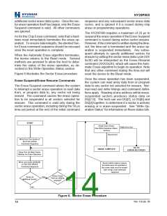
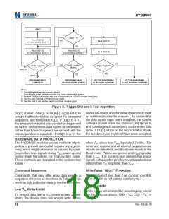
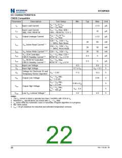
START
DQ[5] = 1?
YES
Read DQ[7:0]
at Valid Address (Note 1)
NO
Read DQ[7:0]
Read DQ[7:0]
Read DQ[7:0]
at Valid Address (Note 1)
Read DQ[7:0]
at Valid Address (Note 1)
YES
NO
DQ[6] Toggled?
(Note 2)
NO
DQ[6] Toggled?
DQ[2] Toggled?
YES
NO
(Note 4)
NO
(Note 3)
YES
PROGRAM/ERASE
COMPLETE
PROGRAM/ERASE
EXCEEDED TIME ERROR
SECTOR BEING READ
IS IN ERASE SUSPEND
SECTOR BEING READ
IS NOT IN ERASE SUSPEND
Notes
:
1. During programming, the program address.
During sector erase, an address within any sector scheduled for erasure.
2. Recheck DQ[6] since toggling may stop at the same time as DQ[5] changes from 0 to 1.
3. Use this path if testing for Program/Erase status.
4. Use this path to test whether sector is in Erase Suspend mode.
Figure 8. Toggle Bit I and II Test Algorithm
device will accept a sector erase data cycle to mark
an additional sector for erasure. To ensure that
the data cycles have been accepted, the system
software should check the status of DQ[3] prior to
and following each subsequent sector erase data
cycle. If DQ[3] is high on the second status check,
the last data cycle might not have been accepted.
DQ[7] (Data# Polling) or DQ[6] (Toggle Bit I) to
ensure that the device has accepted the command
sequence, and then read DQ[3]. If DQ[3] is a ‘1’,
the internally controlled erase cycle has begun and
all further sector erase data cycles or commands
(other than Erase Suspend) are ignored until the
erase operation is complete. If DQ[3] is a ‘0’, the
HARDWARE DATA PROTECTION
The HY29F800 provides several methods of pro-
tection to prevent accidental erasure or program-
ming which might otherwise be caused by spuri-
ous system level signals during VCC power-up and
power-down transitions, or from system noise.
These methods are described in the sections that
follow.
when VCC is less than VLKO (typically 3.7 volts). The
command register and all internal program/erase
circuits are disabled, and the device resets to the
Read mode. Writes are ignored until VCC is greater
than VLKO . The system must provide the proper
signals to the control pins to prevent unintentional
writes when VCC is greater than VLKO
.
Command Sequences
Write Pulse “Glitch” Protection
Commands that may alter array data require a
sequence of cycles as described in Table 5. This
provides data protection against inadvertent writes.
Noise pulses of less than 5 ns (typical) on OE#,
CE# or WE# do not initiate a write cycle.
Logical Inhibit
Low VCC Write Inhibit
Write cycles are inhibited by asserting any one of
the following conditions: OE# = VIL , CE# = VIH, or
To protect data during VCC power-up and power-
down, the device does not accept write cycles
Rev. 4.0/Jan. 00
18

 ETC [ ETC ]