AA2820 PIN DESCRIPTION
OSCILLATOR
PIN
1
NAME
Vdd
DESCRIPTION
Power (+5Vdc)
2
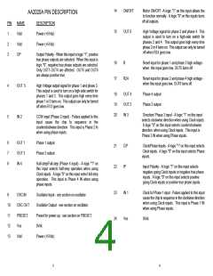
HV OFF
turns high voltage off when logic "0". This does not
reset the high voltage outputs.
Power (+5Vdc)
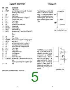
The oscillator frequency must be set at
800kHz to 1.2MHz because of internal
timing. It is strongly recommended to
use the resistor and capacitor values
shown in Figure 5. These values will
produce an oscillator frequency of about
1 Mhz.
3
4
5
6
7
8
9
10
11
12
13
Vdd
OP
Output Polarity
OUT 5
IN 2
OUT 1
OUT 3
IN4
OSC IN
OSC OUT
PRESET
OUT56
high voltage output for phase 1 and phase 3
CCW input/ Phase 2 input
Phase 1 output
Phase 3 output
Half-step/Full-step/ Phase 4 input
Oscillator Input
Oscillator Output
Preset for power up
this output is a logic "1" when both OUT5 and OUT6
are
Figure 5: Oscillator R and C values.
logic "1"
14
15
16
17
18
19
20
21
22
23
24
25
26
27
Vss
Vdd
RUN/STOP
ON/OFF
OUT 6
R13
0Vdc
Power (+5Vdc)
When this input is a logic "0" all clocking is ignored
Motor ON/OFF
high voltage output for phase 2 and phase 4
reset for phase 1 and phase 3 high voltage
reset for phase 2 and phase 4 high voltage
Phase 4 output
Phase 2 output
Direction/ Phase 3 input
Clock/Phase mode
Input polarity
R24
+5V
OUT 4
OUT 2
IN3
C/P
IP
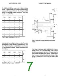
The PRESET pin must be held at
logic "0" upon power up until the
supply for the chip reaches +5V. It is
recommended to use the PRESET
circuit shown in Figure 6. When the
PRESET pin is held at logic "0", all
outputs are off (logic "0"). When the
PRESET pin goes high, the chip
comes up in it's preset condition. In
half-step mode, phase 1 will be on. In
full-step mode, phase 1 and phase 2
will be on.
49.9K
124
1N4448
PRESET
IN 1
Clock In/ Phase 1 input
CLOCK OUT this output gives a pulse for each pulse on the clock
input
0.1uF
10K
or for each phase change when using phase inputs
0Vdc
28
Vss
Figure 6: Preset Circuit.
Inputs in BOLD are available only on the AA2820 SOIC.
7
8

 ETC [ ETC ]