14
15
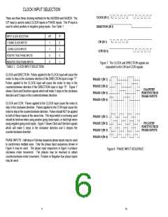
ON/OFF
OUT 6
Motor ON/OFF -A logic "1" on this input allows the
to function normally. A logic "0" on this inputs turns
off all outputs.
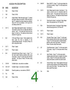
AA2020A PIN DESCRIPTION
DESCRIPTION
PIN
1
NAME
Vdd
High Voltage signal for phase 2 and phase 4. This
output is used to turn on a high-side switch for
phases 2 and 4. This output goes high every time
phase 2 or 4 turns on. This output can only be turned
off when R24 goes low.
Power (+5Vdc)
2
Vdd
Power (+5Vdc)
3
OP
Output Polarity - When this input is logic "1", positive
true phase outputs are selected. When this input is
logic "0", negative true phase outputs are selected.
Only OUT1-OUT4 are affected. OUT5 and OUT6
are always positive true.
16
17
R
Reset input for phase 1 and phase 3 high voltage -
when this input goes low, OUT5 turns off.
R24
Reset input for phase 2 and phase 4 high voltage -
when this input goes low, OUT6 turns off.
4
5
OUT 5
High Voltage output signal for phase 1 and phase 3.
This output is used to turn on a high-side switch for
phases 1 and 3. This output goes high every time
phase 1 or 3 turns on. This output can only be turned
off when R13 goes low.
18
19
20
OUT 4
OUT 2
IN 3
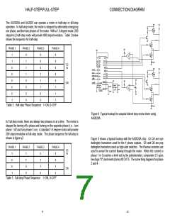
Phase 4 output
Phase 2 output
Direction/ Phase 3 input - A logic "1" on this input
selects clockwise direction when using Clock inputs.
A logic "0" on this input selects counterclockwise
direction when using Clock inputs. This input is
Phase 3 IN when using Phase inputs.
IN 2
CCW input (Phase 2 input) - Pulses applied to this
input cause the chip to sequence in the
counterclockwise direction. This input is Phase 2 In
when using phase inputs.
6
7
8
OUT 1
OUT 3
IN 4
Phase 1 output
Phase 3 output
21
22
C/P
IP
Clock/Phase Inputs - A logic "1" on this input selects
Clock inputs. A logic "0" on this input selects Phase
inputs.
Half-step/Full-step (Phase 4 input) - A logic "1" on
this input selects half-step operation when using
Clock inputs. A logic "0" on this input select full-step
operation. This input is Phase 4 IN when using
phase inputs.
Input Polarity - A logic "1" on this input selects
negative going Clock inputs or negative true phase
inputs. A logic "0" on this input selects positive
going Clock inputs or positive true phase inputs.
23
24
IN 1
Vss
Clock In/ Phase 1 input - Pulses applied to this input
cause the chip to sequence in the clockwise direction
when using Clock inputs. This input is Phase 1 IN
when using Phase inputs.
9
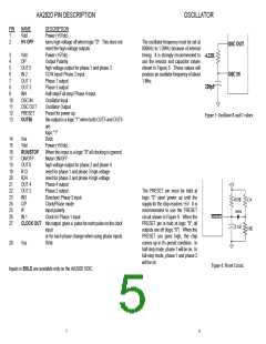
OSC IN
Oscillator Input - see section on oscillator.
10
11
12
13
OSC OUT
PRESET
Vss
Oscillator Output - see section on oscillator.
Preset for power up - see section on PRESET
0Vdc
0Vdc
Vdd
Power (+5Vdc)
5
6

 ETC [ ETC ]