Proprietary TranSwitch Corporation Information for use Solely by its Customers
L3M
TXC-03452B
DATA SHEET
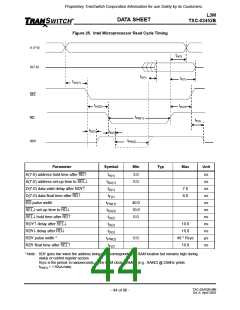
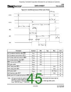
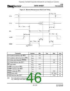
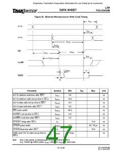
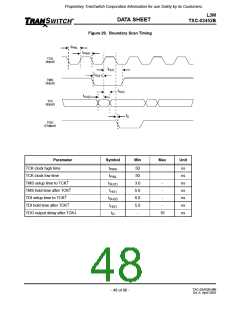
Figure 25. Intel Microprocessor Read Cycle Timing
A (7-0)
D(7-0)
tH(1)
tD(1)
tF(1)
tSU(1)
SEL
RD
tSU(2)
tH(2)
tPW(1)
tF(2)
tD(2)
tD(3)
tPW(2)
RDY
Parameter
Symbol
Min
Typ
Max
Unit
A(7-0) address hold time after RD↑
A(7-0) address set-up time to SEL↓
D(7-0) data valid delay after RDY↑
D(7-0) data float time after RD↑
RD pulse width
tH(1)
tSU(1)
tD(1)
3.0
0.0
ns
ns
ns
ns
ns
ns
ns
ns
ns
µs
ns
7.0
tF(1)
6.0
tPW(1)
tSU(2)
tH(2)
40.0
10.0
0.0
SEL↓ set-up time to RD↓
SEL↓ hold time after RD↑
RDY↑ delay after SEL↓
tD(2)
10.0
16.0
RDY↓ delay after RD↓
tD(3)
RDY pulse width *
tPW(2)
tF(2)
0.0
48 * Rcyc
10.0
RDY float time after SEL↑
* Note: RDY goes low when the address being read corresponds to a RAM location but remains high during
status or control register access.
Rcyc is the period, in nanoseconds, of the RAM clock (RAMCI) (e.g., RAMCI @ 25MHz yields
tPW(2) = 1.92µs max)
TXC-03452B-MB
Ed. 6, April 2001
- 44 of 96 -

 ETC [ ETC ]