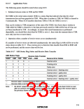
9. Cautions on Switching of SCK3X Pin Function
If the function of the SCK3X pin is switched from clock output to I/O port after using the SCI3 in
clock synchronization mode, the “low” level is output in a moment (1/2 of the system clock ø) at
the SCK3X pin function switching.
This momentary “low” level output can be avoided in either of the following two methods:
a. When disabling SCK3X pin clock output
When stopping signal transmission, clear the bits TE and RE in SCR3, and set the CKE1
bit to “1” and the CKE0 bit to “0” simultaneously with a single command.
In this case, use the COM bit in SMR set at “1”. This means it cannot be used as an I/O
port. Also, to avoid intermediate potential from being applied to the SCK3X pin, pull up the
line connected to the SCK3X pin to VCC potential with a resistance, or supply an output from
other devices.
b. When switching the SCK3X pin function from clock output to I/O port
When stopping signal transmission,
(1) Clear the bits TE and RE in SCR3, and set the CKE1 bit to “1” and the CKE0 bit to “0”
simultaneously with a single command.
(2) Then, clear the COM bit in SMR to “0”.
(3) Finally, clear the bits CKE1 and CKE0 in SCR3 to “0”. Avoid intermediate potential
from being applied to the SCK3X pin.
10. Setting in Subactive and Subsleep Modes
In subactive or subsleep mode, SCI3 can be used only when the øW/2 is selected as the CPU clock.
Set the SA1 bit in SYSCR2 to “1”.
323

 ETC [ ETC ]