3. Break detection and processing
When a framing error is detected, a break can be detected by reading the value of the RXD3X pin
directly. In a break, the input from the RXD3X pin becomes all 0s, with the result that bit FER is
set and bit PER may also be set.
SCI3 continues the receive operation even after receiving a break. Note, therefore, that even
though bit FER is cleared to 0 it will be set to 1 again.
4. Mark state and break detection
When bit TE is cleared to 0, the TXD3X pin functions as an I/O port whose input/output direction
and level are determined by PDR and PCR. This fact can be used to set the TXD3X pin to the mark
state, or to detect a break during transmission.
To keep the communication line in the mark state (1 state) until bit TE is set to 1, set PCR = 1 and
PDR = 1. Since bit TE is cleared to 0 at this time, the TXD3X pin functions as an I/O port and 1 is
output.
To detect a break, clear bit TE to 0 after setting PCR = 1 and PDR = 0.
When bit TE is cleared to 0, the transmission unit is initialized regardless of the current
transmission state, the TXD3X pin functions as an I/O port, and 0 is output from the TXD3X pin.
5. Receive error flags and transmit operation (synchronous mode only)
When a receive error flag (OER, PER, or FER) is set to 1, transmission cannot be started even if
bit TDRE is cleared to 0. The receive error flags must be cleared to 0 before starting transmission.
Note also that receive error flags cannot be cleared to 0 even if bit RE is cleared to 0.
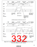
6. Receive data sampling timing and receive margin in asynchronous mode
In asynchronous mode, SCI3 operates on a basic clock with a frequency 16 times the transfer rate.
When receiving, SCI3 performs internal synchronization by sampling the falling edge of the start
bit with the basic clock. Receive data is latched internally at the 8th rising edge of the basic clock.
This is illustrated in figure 10-26.
320

 ETC [ ETC ]