3. Pin configuration
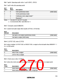
Table 10-2 shows the SCI1 pin configuration.
Table 10-2 SCI1 Pin Configuration
Name
Abbrev.
SCK1
SI1
I/O
Function
SCI1 clock
I/O
SCI1 clock input/output
SCI1 receive data input
SCI1 transmit data output
SCI1 data input
SCI1 data output
Input
Output
SO1
4. Register configuration
Table 10-3 shows the SCI1 register configuration.
Table 10-3 Registers
Name
Abbrev.
SCR1
R/W
R/W
R/W
R/W
R/W
R/W
Initial Value
H'00
Address
Serial control register 1
Serial control status register 1
Serial data register U
Serial data register L
Clock stop register 1
H'FFA0
H'FFA1
H'FFA2
H'FFA3
H'FFFA
SCSR1
SDRU
H'9C
Undefined
Undefined
H'FF
SDRL
CKSTPR1
10.2.2
Register Descriptions
1. Serial control register 1 (SCR1)
Bit
7
SNC1
0
6
5
4
3
2
1
0
CKS0
0
SNC0 MRKON LTCH
CKS3
0
CKS2
0
CKS1
0
Initial value
Read/Write
0
0
0
R/W
R/W
R/W
R/W
R/W
R/W
R/W
R/W
SCR1 is an 8-bit read/write register that controls the operating mode, serial clock source, and
prescaler division ratio.
Upon reset, SCR1 is initialized to H'00. If this register is written to during transfer, transfer will be
halted.
254

 ETC [ ETC ]