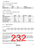
5. Clock stop register 1 (CKSTPR1)
7
6
5
4
3
2
1
0
Bit:
S1CKSTP S31CKSTP S32CKSTP ADCKSTP TGCKSTP TFCKSTP TCCKSTP TACKSTP
1
1
1
1
1
1
1
Initial value:
Read/Write:
1
R/W
R/W
R/W
R/W
R/W
R/W
R/W
R/W
CKSTPR1 is an 8-bit read/write register that performs module standby mode control for peripheral
modules. Only the bit relating to timer G is described here. For details of the other bits, see the
sections on the relevant modules.
Bit 3: Timer G module standby mode control (TGCKSTP)
Bit 3 controls setting and clearing of module standby mode for timer G.
TGCKSTP
Description
0
1
Timer G is set to module standby mode
Timer G module standby mode is cleared
(initial value)
9.5.3
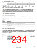
Noise Canceler
The noise canceler consists of a digital low-pass filter that eliminates high-frequency component
noise from the pulses input from the input capture input pin. The noise canceler is set by NCS* in
PMR3.
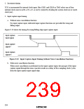
Figure 9-8 shows a block diagram of the noise canceler.
Sampling
clock
C
C
C
C
C
Input capture
input signal
D
Q
D
Q
D
Q
D
Q
D
Q
Noise
canceler
output
Latch
Latch
Latch
Latch
Latch
Match
detector
∆t
Sampling clock
∆t: Set by CKS1 and CKS0
Figure 9-8 Noise Canceler Block Diagram
221

 ETC [ ETC ]