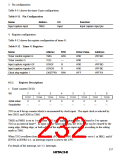
3. Pin configuration
Table 9-11 shows the timer G pin configuration.
Table 9-11 Pin Configuration
Name
Abbrev.
I/O
Function
Input capture input
TMIG
Input
Input capture input pin
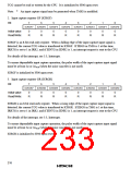
4. Register configuration
Table 9-12 shows the register configuration of timer G.
Table 9-12 Timer G Registers
Name
Abbrev.
TMG
R/W
R/W
—
Initial Value
Address
H'FFBC
—
Timer control register G
Timer counter G
H'00
H'00
H'00
H'00
H'FF
TCG
Input capture register GF
Input capture register GR
Clock stop register 1
ICRGF
ICRGR
CKSTPR1
R
H'FFBD
H'FFBE
H'FFFA
R
R/W
9.5.2
Register Descriptions
1. Timer counter (TCG)
7
6
5
4
3
TCG3
0
2
TCG2
0
1
0
Bit:
TCG7
TCG6
TCG5
TCG4
TCG1
0
TCG0
0
0
0
0
Initial value:
Read/Write:
0
—
—
—
—
—
—
—
—
TCG is an 8-bit up-counter which is incremented by clock input. The input clock is selected by
bits CKS1 and CKS0 in TMG.
TMIG in PMR1 is set to 1 to operate TCG as an input capture timer, or cleared to 0 to operate
TCG as an interval timer*. In input capture timer operation, the TCG value can be cleared by the
rising edge, falling edge, or both edges of the input capture input signal, according to the setting
made in TMG.
When TCG overflows from H'FF to H'00, if OVIE in TMG is 1, IRRTG is set to 1 in IRR2, and if
IENTG in IENR2 is 1, an interrupt request is sent to the CPU.
For details of the interrupt, see 3.3, Interrupts.
217

 ETC [ ETC ]