APEX 20K Programmable Logic Device Family Data Sheet
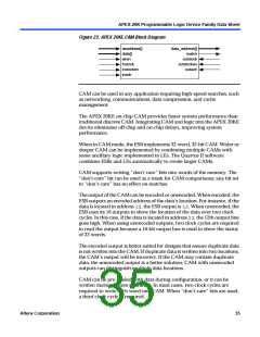
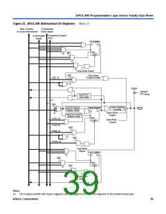
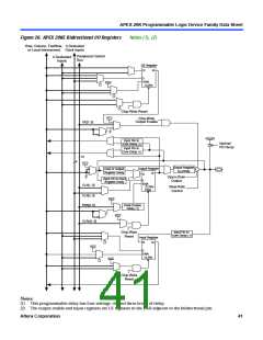
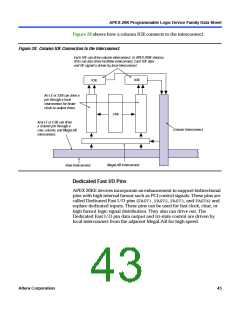
Figure 25. APEX 20K Bidirectional I/O Registers Note (1)
Row, Column,
or Local Interconnect Clock Inputs
2 Dedicated
Peripheral Control
Bus
4 Dedicated
Inputs
OE Register
D
Q
ENA
VCC
CLRN
Chip-Wide Reset
VCC
Chip-Wide
Output Enable
OE[7..0]
VCCIO
Optional
PCI Clamp
Input Pin to
Core Delay
12
2
VCC
Output Register
Delay
Output Register
Core to Output
Register Delay
t
CO
Q
D
Open-Drain
Output
Input Pin to Input
Register Delay
ENA
CLRN
CLK[1..0]
Slew-Rate
Control
CLK[3..2]
ENA[5..0]
VCC
VCC
CLRn[1..0]
Chip-Wide
Reset
Input Register
D
Q
VCC
ENA
CLRN
VCC
Chip-Wide
Reset
Note:
(1) The output enable and input registers are LE registers in the LAB adjacent to the bidirectional pin.
Altera Corporation
39

 ETC [ ETC ]