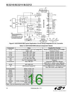
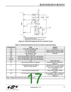
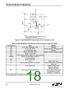
Si3210/Si3211/Si3212
QRDN
QTDN
5401
Q3
Q4
5401
R23
R24
RRBN0
3.0k
RTBN0
3.0k
QRP
5551
QTN
5551
Q5
Q6
C8
C7
CRBN
100 nF
CTBN
100 nF
R7
RRE
80.6
R12
RRBN
5.1k
R6
RTE
80.6
R13
RTBN
5.1k
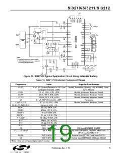
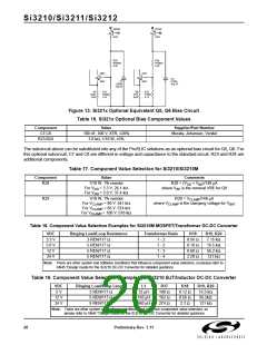
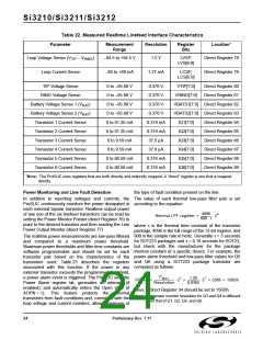
Figure 13. Si321x Optional Equivalent Q5, Q6 Bias Circuit
Table 16. Si321x Optional Bias Component Values
Component
C7,C8
Value
Supplier/Part Number
Murata, Johanson, Venkel
100 nF, 100 V, X7R, ±20%
3.0 kΩ, 1/10 W, ±5%
R23,R24
The subcircuit above can be substituted into any of the ProSLIC solutions as an optional bias circuit for Q5, Q6. For
this optional subcircuit, C7 and C8 are different in voltage and capacitance to the standard circuit. R23 and R24 are
additional components.
Table 17. Component Value Selection for Si3210/Si3210M
Component
Value
Comments
R28 = (V + V )/148 µA
R28
1/10 W, 1% resistor
DD
BE
For V = 3.3 V: 26.1 kΩ
where V is the nominal VBE for Q9
DD
BE
For V = 5.0 V: 37.4 kΩ
DD
R29
1/10 W, 1% resistor
R29 = V
/148 µA
CLAMP
For V
For V
For V
= 80 V: 541 kΩ
= 85 V: 574 kΩ
= 100 V: 676 kΩ
where V
is the clamping voltage for V
CLAMP
CLAMP
CLAMP
CLAMP BAT
Table 18. Component Value Selection Examples for Si3210M MOSFET/Transformer DC-DC Converter
VDC
3.3 V
5.0 V
12 V
24 V
Ringing Load/Loop Resistance
3 REN/117 Ω
Transformer Ratio
R18
R19, R20
7.15 kΩ
16.5 kΩ
56.2 kΩ
121 kΩ
1 - 2
1 - 2
1 - 3
1 - 4
0.56 Ω
0.10 Ω
0.68 Ω
2.20 Ω
5 REN/117 Ω
5 REN/117 Ω
5 REN/117 Ω
Note: There are other system and software conditions that influence component value selection, so please refer to
AN45 “Design Guide for the Si3210 DC-DC Converter for detailed guidance.
Table 19. Component Value Selection Examples for Si3210 BJT/Inductor DC-DC Converter
VDC
5 V
Ringing Load/Loop Length
3 REN/117 Ω
L1
R17
R18
R19, R20
16.5 kΩ
56.2kΩ
121 kΩ
33 µH
150 µH
560 µH
100 Ω
162 Ω
274 Ω
0.12 Ω
0.56 Ω
2.2 Ω
12 V
24 V
5 REN/117 Ω
5 REN/117 Ω
Note: There are other system and software conditions that influence component value selection, so
please refer to AN45 “Design Guide for the Si3210 DC-DC Converter for detailed guidance.
20
Preliminary Rev. 1.11

 ETC [ ETC ]