PRELIMINARY
PCT1789W DATA SHEET
PCT303DW CONTROL REGISTERS
!!
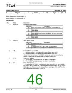
Daisy-Chain Control
(Register 14, R/W)
NSLV[2:0]
SSEL[1:0]
FSD
RPOL
DCE
7
6
5
4
3
2
1
0
Reset settings: 02h (serial mode 0,1)
Reset settings: 3Fh (serial mode 2)
Bit Definitions:
Bits
Name
Description
7:5
NSLV[2:0]
Number of slave devices.
NSLV[2:0]
Description
000
001
010
011
100
101
110
111
0 slave devices. Simply redefines the FC/RGDT and RGDT/FSD pins.
1 slave device.
2 slave devices.
3 slave devices.
4 slave devices. For four or more slave devices, the FSD bit MUST be set.
5 slave devices.
6 slave devices.
7 slave devices.
4:3
SSEL[1:0]
Slave device select.
SSEL[1:0]
Description
00
01
10
11
16-bit SDO receive data.
Reserved.
15-bit SDO receive data. LSB = 1 for the PCT303DW device.
15-bit SDO receive data. LSB = 0 for the PCT303DW device.
2
FSD
Delayed frame sync control.
1 = Sets the number of SCLK periods between frame syncs to 16.
0 = Sets the number of SCLK periods between frame syncs to 32.
This bit MUST be set when PCT303DW devices are used as slaves. For the
master PCT303DW, only serial mode 1 is allowed in this case.
1
0
RPOL
DCE
Ring detect polarity.
1 = The FC/RGDT pin (operating as ring detect) is active-high.
0 = The FC/RGDT pin (operating as ring detect) is active-low.
Daisy-chain enable.
1 = Enables the PCT303DW to operate with slave devices on the same serial
bus. The FC/RGDT signal (pin 7) becomes the ring detect output and the RGDT/
FSD signal (pin 15) becomes the delayed frame sync signal. Note that ALL other
bits in this register are ignored if DCE = 0.
PRELIMINARY
PC-TEL, Inc.
46
1789W0DOCDAT06A-0299

 ETC [ ETC ]