PCT1789W DATA SHEET
PRELIMINARY
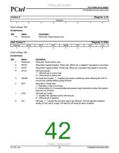
PCT303DW CONTROL REGISTERS
!!
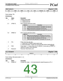
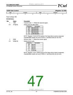
DAA Control 2
(Register 6, R/W)
CPE
ATM1
ARM1
PDL
PDN
Reserved
ATM0
ARM0
7
6
5
4
3
2
1
0
Reset settings: 70h
Bit Definitions:
Bits
Name
CPE
Description
7
Charge pump enable.
1 = Charge pump on.
0 = Charge pump off.
6,1
ATM[1:0]
ARM[1:0]
PDL
AOUT transmit path level control.
ATM[1:0]
Description
00
01
10
11
–20dB transmit path attenuation for call progress AOUT pin only.
–32dB transmit path attenuation for call progress AOUT pin only.
Mutes transmit path for call progress AOUT pin only.
–26dB transmit path attenuation for call progress AOUT pin only.
5,0
AOUT receive path level control.
ARM[1:0]
Description
00
01
10
11
0dB receive path attenuation for call progress AOUT pin only.
–12dB receive path attenuation for call progress AOUT pin only.
Mutes receive path for call progress AOUT pin only.
–6dB receive path attenuation for call progress AOUT pin only.
4
Power down line-side chip.
1 = Places the PCT303W in lower power mode.
0 = Normal operation. Program the clock generator before clearing this bit.
3
2
PDN
Power down. 1 = Powers down the PCT303DW. A reset pulse on RESET is
required to restore normal operation.
Reserved
Reserved. Read returns zero.
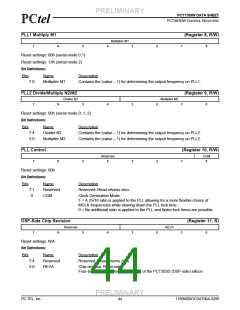
PLL1 Divide N1
(Register 7, R/W)
Divider N1
7
6
5
4
3
2
1
0
Reset settings: 00h (serial mode 0, 1, 2)
Bit Definitions:
Bits
Name
Description
7:0
Divider N1
Contains the (value – 1) for determining the output frequency on PLL1.
PRELIMINARY
PC-TEL, Inc.
43
1789W0DOCDAT06A-0299

 ETC [ ETC ]