PRELIMINARY
PCT1789W DATA SHEET
PCT303DW CONTROL REGISTERS
!!
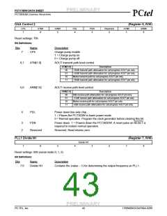
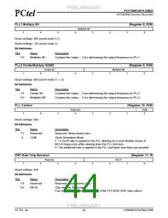
PLL1 Multiply M1
(Register 8, R/W)
Multiplier M1
7
6
5
4
3
2
1
0
Reset settings: 00h (serial mode 0,1)
Reset settings: 13h (serial mode 2)
Bit Definitions:
Bits
Name
Description
Contains the (value – 1) for determining the output frequency on PLL1.
7:0
Multiplier M1
PLL2 Divide/Multiply N2/M2
(Register 9, R/W)
Divider N2
Multiplier M2
7
6
5
4
3
2
1
0
Reset settings: 00h (serial mode 0, 1, 2)
Bit Definitions:
Bits
Name
Description
7:4
3:0
Divider N2
Multiplier M2
Contains the (value – 1) for determining the output frequency on PLL2.
Contains the (value – 1) for determining the output frequency on PLL2.
PLL Control
(Register 10, R/W)
Reserved
CGM
7
6
5
4
3
2
1
0
Reset settings: 00h
Bit Definitions:
Bits
Name
Description
7:1
0
Reserved
CGM
Reserved. Read returns zero.
Clock Generation Mode.
1 = A 25/16 ratio is applied to the PLL allowing for a more flexible choice of
MCLK frequencies while slowing down the PLL lock time.
0 = No additional ratio is applied to the PLL and faster lock times are possible.
DSP-Side Chip Revision
(Register 11, R)
Reserved
REVA
7
6
5
4
3
2
1
0
Reset settings: N/A
Bit Definitions:
Bits
Name
Description
7:4
3:0
Reserved
REVA
Reserved. Read returns zero.
Chip revision. Read-only.
Four-bit value indicating the revision of the PCT303D (DSP-side) silicon.
PRELIMINARY
PC-TEL, Inc.
44
1789W0DOCDAT06A-0299

 ETC [ ETC ]